INT. J. ELECTRONICS, 1993, VOL. 74, NO. 3, 407-410
Optimal linewidth distribution minimizing average signal delay for RC
limited circuits
HALDUN M. OZAKTASt and JOSEPH W. GOODMANt
Based on idealized interconnect scaling rules, we derive the optimal distribution of linewidths as a function of length for wire-limited layouts utilizing RC-limited interconnections. We show that the width of the wires should be chosen propor tional to the cube root of their length for two-dimensional layouts and propor tional to the fourth root of their length for full three-dimensional layouts so as to minimize average signal delay.
Circuit layouts where the packing density is limited by the finite widths of the wires (Keyes 1982) are considered. We further limit our attention to the case where the signal delay along a particular line of length / is given by r(/)=RC/2, the rise
time of the line. R and C are the resistance and capacitance, respectively, of the line
per unit length. Thus we assume that the line is neither drive nor propagation limited.
The cross-section of such a line is shown in Fig. l. Alternate geometries (stripline, coax, etc.) can also be used and would not affect the results. We assume that the ratios between all quantities in the figure are kept constant as we scale the line, i.e. the line is scaled photographically. This approach keeps the characteristic impedance and capacitance per unit length of the lines constant as they are scaled.
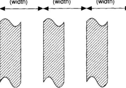
(width) denotes the transverse extent allocated for a single line, including its share of line-to-line separations (Fig. 2). The fixed ratio between (width) and w is set by
cross-w (height) conductor (width) t h
Figure 1. Cross-section of an interconnection. We assume that the ratios between all dimensions are kept fixed for all lines.
Received 25 February 1992; revised 28 March 1992; accepted 30 April 1992. Communi cated by H. L. Hartnagel.
t
Department of Electrical Engineering, Bilkent University, 06533 Bilkent, Ankara, Turkey.tDepartment of Electrical Engineering, Stanford University, Stanford, CA 94305, U.S.A.
408 H. M. Ozaktas and J. W. Goodman
(width) (width) (width)
...
...
...
..
Figure 2. Top view of several interconnections. (width) denotes transverse extent allocated
for a single line, including its share of line-to-line separations. Thus L/(width) lines can
pass through a spacing of width L. (height) has a similar interpretation for hypothetical
three-dimensional layouts. S/(width)(height) lines can pass through a surface of area S.
Thus these parameters define the packing density of the lines.
talk considerations (the dependence of cross-talk on length is ignored). Similarly,
(width) x (height) denotes the transverse cross-sectional area devoted to a single line.
Since a fixed (width)/(height) ratio is also maintained the cross-sectional area is oc (width)2. Since the skin effect need not be considered (Solomon 1982), the series
resistance per unit length R is proportional to oc 1/wt oc l/w2 oc I/(width)2• Thus the
rise time may be written as
[2
r(/)
=
RC/2=
K (width)2 (1)since the capacitance per unit length C is constant. The constant K can be minimized by an appropriate choice of the ratios w/h, w/t, (width)/w, etc. and also involves the resistivity of the conducting material and the permittivity of the dielectric material. We will assume that different lines in the same system can be scaled independently according to our scaling scheme. It should be noted that this is not possible with present VLSI technology since t and h are fixed for all lines in the same layer, a point to which we will return later.
We consider a cartesian grid of N primitive devices spaced apart at an, as yet undetermined, lattice spacing d (Keyes 1982). Thus, any physical length l may be written as l = rd where r is the length in grid units. First consider a two-dimensional array of N 112 x N 112 devices. The area occupied by a wire of length l = rd is just
rd(width(r)) where (width(r)) denotes the transverse extent allocated for a line of
length r. Since we assume a wiring area limited system, we equate the total area occupied by all wires to the total wiring area available in the assumed M layers (Keyes 1982):
N
f��·
[rd(width(r))]g(r)dr=MNd2 (2)where g(r) is the line length distribution (Gardner et al. 1987). That is, g(r)tir gives the expected number of lines per device with lengths lying in the interval [r, r
+
Ar].Thus, k= Jg(r) dr is the average number of lines per device. We assume rmax� 1 so
Optimal linewidth distribution for RC circuits 409 inefficiency factors arising from imperfect utilization of the wiring area can be absorbed in the definition of M. Also note that our model does not account for multiple signal nets. Using r:(r)=Kr2d2/(width(r))2 and solving ford from (2), we
can obtain the average rise time as: •ave=i f r:(r)g(r) dr=K' [
f(wid;�(r))2 g(r) dr
J [
f r(width)(r))g(r) dr J (3)where K'=K/(kM2). All integrals are from r=l to r
max- Using the standard
techniques of the calculus of variations, the functional form of (width(r)) minimizing rave may be shown to be (see the Appendix):
( width(r))
=
Awr113 (4)where Aw is an arbitrary constant. The same procedure can be repeated for full three
dimensional layouts by equating the total system volume to the total volume occupied by the wires. We now find that the optimal functional form is:
( width(r))
=
Awr114 (5)If a full three-dimensional layout cannot be built, we would expect partially or quasi-three dimensional layouts to have optimal linewidth distributions with an exponent lying between l/3 and l/4.
The arbitrariness of Aw arises from the scale invariance of wire-limited RC
systems (Masaki 1989), i.e. the system can be photographically scaled within certain bounds without effecting the delay. Depending on the choice of Aw, it may not be
possible to manufacture the shortest lines as narrow as dictated by (4). If Aw is too
small, this will affect a large fraction of the lines so that our results will not be applicable. On the other hand, if Aw is too large, it will not be accurate to ignore
inductive effects, the lines may become propagation-limited, rather than RC-limited. Thus, Aw must be set to an appropriate intermediate value. If the minimum
manufacturable linewidth is not small enough, there may not be a suitable choice of Aw which is not affected by either of these considerations.
In conclusion, we see that it is optimal to construct longer lines sub-linearly wider, as given by (4) and (5). The optimal linewidth distribution is independent of g(r), the line length distribution. Some insight as to this result can be gained by substituting (4) directly into (3). This reduces both the integrals in (3) to the form Jr413g(r)dr. Readers experienced in variational problems might have guessed that
the optimal form of(width(r)) would be that which equates these two integrals for all g(r) (within a constant factor). Thus with r2g(r)/(width(r))2 oc rg(r)(width(r)) they
would obtain (width(r)) oc r113• We see that (width(r)) does not depend on g(r) since g(r) cancels from this equality.
In practice, it would probably not be feasible to continuously contour the linewidth as a function of line length, so that a staircase approximation to (4) could be used instead. Real computing systems are built out of a hierarchy of different technologies, each higher level employing wider lines. Thus, apart from their theoretical interest, the presented results may be useful as a guideline in contemplat ing the inter-connection hierarchy when minimization of average signal delay is an objective.
410 Optimal linewidth distribution for RC circuits
We mentioned that our scaling rules cannot be applied to the lines of present day VLSI chips because h and t are fixed for all lines in the same layer. This is not
optimal. However, many-layer technolgies are becoming available. Thus the upper layers which are reserved for the longer and wider wires may be constructed with larger values of h and t in accordance with our scaling rules. Then, a staircase
approximation to (4) is possible. Thus, the presented results may also be used as a guideline in the construction of future many-layer ULSI, WSI or hybrid SWI circuits.
Appendix
Here we sketch the derivation of (4) from (3). Formal details of such standard procedures may be found in the textbooks (Hildebrand 1965). The first step is to substitute (width(r) )--+(width(r)) + e17(r) in (3). Here 17(r) is an arbitrary well behaved function and e a small number. If (width(r)) is to minimize 'ave• the first-order
variation of 'ave with respect to (width(r)) must vanish. (Note the analogy with usual
differential calculus. If a function has a minimum at a certain point, its first-order variation about that point vanishes .) e acts as a parameter of this variation. Thus 8,ave/8e must vanish ate= 0. After performing the above substitution, differentiation
with respect to e, letting e
=
0 and equating to zero, we find that the optimum form of (width(r)) must satisfy:[ f
r2g(r) drJ [
r
J [
(r211(r)g(r) dr] [
r
.J
J(width(r))2 J'17(r)g(r)dr =
J
(width(r))3 J'(width(r))g(r)drwhich can be written as:
I{
'[
f
r2g(r) drJ
r'2 [r
.
]}
I I I r J(width(r))2 -(width(r'))3 J'(wzdth(r))g(r)dr 17(r )g(r )dr =0(6)
(7) Since 17(r) is arbitrary, the expression inside the curly brackets must be identically equal to zero. Thus:
'[
r
r2g(r)drJ ,
12
[
r
.
J
r J (width(r) )2 = (width(r') )3 J'(wzdth(r) )g(r) dr (8) The solution of this equation is (width(r))=Awr113, as can be easily verified by direct
substitution. This last step also reveals that g(r) has no effect and that the choice of Am is arbitrary. Since it proceeds along similar lines, the derivation of (5) is not
presented.
REFERENCES
GARDNER, D. S., MEINDL, J. D., and SARASWAT, K. C., 1987, Interconnection and electro migration scaling theory. I.E.E.E. Transactions on Electron Devices, 34, 633-643.
HILDEBRAND, F. B., 1965, Methods of Applied Mathematics (Englewood Cliffs, NJ: Prentice
Hall).
KEYES, R. W., 1982, The wire-limited Jog chip. I.E.E.E. Journal of Solid State Circuits, 17, 1232-1233.
MASAKI, A., 1989, Electrical resistance as a limiting factor for high performance: computer packaging. I.E.E.E. Circuits and Devices Magazine, 22-26.
SOLOMON, P. M., 1982, A comparison of semiconductor devices for high speed logic. Proceedings of the Institute of Electrical and Electronics Engineers, 70, 489-509.