Comparative study of electroabsorption in InGaN / GaN quantum zigzag
heterostructures with polarization-induced electric fields
Emre Sari,1,2,3Tuncay Ozel,2,3,4Aslı Koc,2,3Jin-Woo Ju,5Haeng-Keun Ahn,5 In-Hwan Lee,5Jong-Hyeob Baek,6and Hilmi Volkan Demir1,2,3,4,a兲
1
Department of Electrical and Electronics Engineering, Bilkent University, Ankara TR-06800 Bilkent, Turkey
2
Nanotechnology Research Center, Bilkent University, Ankara TR-06800 Bilkent, Turkey
3
Institute of Materials Science and Nanotechnology, Bilkent University, Ankara TR-06800 Bilkent, Turkey
4
Department of Physics, Bilkent University, Ankara TR-06800 Bilkent, Turkey
5
School of Advanced Materials Engineering, Research Center of Industrial Technology, Chonbuk National University, Chonju 561-756, Republic of Korea
6
Korea Photonics Technology Institute, Gwangju 500-460, Republic of Korea
共Received 2 April 2008; accepted 29 April 2008; published online 19 May 2008兲
We present a comparative study on InGaN/GaN quantum zigzag structures embedded in p-i-n diode architecture that exhibit blue-shifting electroabsorption in the blue when an electric field is externally applied to compensate for the polarization-induced electric field across the wells. With the polarization breaking their symmetry, the same InGaN/GaN quantum structures redshift their absorption edge when the external field is applied in the same direction as the well polarization. Both computationally and experimentally, we investigate the effects of polarization on electroabsorption by varying compositional content and structural parameters and demonstrate that electroabsorption grows stronger with weaker polarization in these multiple quantum well modulators. © 2008 American Institute of Physics.关DOI:10.1063/1.2931696兴
An important, distinctive property of III-nitride quantum heterostructures is the formation of strong polarization when they are grown on the c plane of their wurtzite crystal structure.1 Due to the discontinuity of polarization with abrupt compositional changes at the heterointerfaces of such III-N multiple quantum wells 共MQWs兲, large electrostatic fields in alternating directions are induced across the well/ barrier pairs. As a result, the band structure of these MQWs yields zigzag potential profiles in conduction and valence bands instead of conventional square potential profiles. This substantially alters electric field dependence of optical ab-sorption in III-N MQW structures.
Electroabsorption measurements are also essentially in-formative to understand the underlying physics behind such polar III-N structures. We previously demonstrated a quan-tum electroabsorption modulator based on InGaN/GaN quantum zigzag structures operating in the blue2 and in the near-ultraviolet.3In the previous work of our group and oth-ers, however, the effect of polarization on electroabsorption in polar InGaN/GaN has not been comparatively studied or systematically investigated to date.2–4 To this end, in this letter, we present the design, growth, fabrication, experimen-tal characterization, and theoretical analysis of InGaN/GaN quantum zigzag structures with different levels of polarization-induced electrostatic fields that are set by con-trolling the alloy content and well-to-barrier width ratio. In this work, we comparatively study the effects of polarization-induced electrostatic field on the performance of our quantum electroabsorption modulators and develop a better understanding to design devices for stronger electro-absorption.
Polarization in III-nitrides consists of piezoelectric and spontaneous components. The discontinuity of the total po-larization causes accumulation of very high density 共⬃1013cm−2兲, two-dimensional electron gas 共2DEG兲 and 2D hole gas 共2DHG兲 at the heterointerfaces.5 Moreover, in MQW structures, the alternating sign of 2D charge densities in the well-to-barrier and barrier-to-well heterointerfaces re-sults in built-in electrostatic fields that also alternate in direction.1 These polarization-induced built-in electrostatic fields across the wells and the barriers are expressed in Eqs. 共1兲 and共2兲, respectively, such that there is no voltage build up across the whole MQW structure. Here, spontaneous and piezoelectric polarization for any periodic MQW structure formed in InAlGaN alloys can be calculated using the mate-rial parameters of InN, AlN, and GaN with a first order in-terpolation. As evident from Eqs. 共1兲 and 共2兲, besides the well and barrier alloy content, the built-in electrostatic field depends on the well-to-barrier width ratio.
Etotwell= Espwell+ Epzwell=共Psp barrier
+ Ppzbarrier兲 − 共Pspwell+ Ppzwell兲
⑀well+ dwell dbarrier ⑀barrier . 共1兲 Etotbarrier= Espbarrier+ Epzbarrier
=共Psp well
+ Ppzwell兲 − 共Pspbarrier+ Ppzbarrier兲
⑀barrier+ dbarrier
dwell ⑀well
. 共2兲
For our comparative study, we designed three sets of InGaN/GaN quantum structures incorporated in a p-i-n di-ode architecture. Among these sets, the structural parameters of their active regions were carefully selected for comparison purposes. These structural parameters include InN concentra-a兲Author to whom correspondence should be addressed. Electronic mail:
[email protected]. Tel.:关⫹90兴共312兲 1021. FAX: 关⫹90兴共312兲 290-1015.
APPLIED PHYSICS LETTERS 92, 201105共2008兲
tions in the quantum well regions and well-to-barrier width ratios. We used a generic p-i-n epitaxial design for these three sets of samples共samples A, B, and C兲. In our design, we included five quantum well/barrier pairs for all of the structures. Sample A was designed to have an active MQW layer of 2.5 nm/7.5 nm In0.15Ga0.85N/GaN quantum well/ barrier structures. Sample B has the same structure with 3 nm/4 nm In0.15Ga0.85N/GaN and Sample C with 3 nm/4 nm In0.12Ga0.88N/GaN. These epistructures were de-signed to study only the polarization effect varied through these two parameters. Using the design and material param-eters of GaN and InN, we calculate built-in electrostatic fields inside the well and barrier layers of samples A, B, and
C. The polarization-induced electric field across the wells
were set to be −383 V/m for sample A, −300 V/m for sample B, and −238 V/m for sample C, while those across the barriers were set to be 127 V/m for sample A, 220 V/m for sample B, and 179 V/m for sample C.
We grew these epitaxial structures using a metal organic chemical vapor deposition system on c-plane sapphire sub-strates. We used exactly the same conditions for the epitaxial growth of all samples except for their active layers. We tuned InN incorporation into the MQW layers by changing the growth temperature and their layer thickness by changing the growth time of each layer. Detailed growth conditions can be found elsewhere.6 Following the epitaxial growth, we fabri-cated diode mesas with electrodes using reactive ion etching,
p and n contact metallization, and annealing steps.2,3 The three samples in this work were all fabricated using our stan-dard semiconductor processes7–9 and then characterized un-der the same conditions. We performed photoluminescence 共PL兲 and double crystal x-ray diffraction 共DCXRD兲 measure-ments to verify the growth of the desired quantum structures with the intended alloy content and high crystal quality. PL spectra for these samples were obtained using a He–Cd laser at an excitation wavelength of 325 nm. PL peaks at 450, 450, and 425 nm for samples A, B, and C, respectively, verify the growth of the InGaN quantum wells within 1.5% of the de-sired InN ratio.
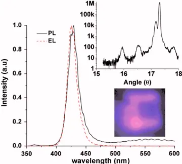
Figure 1 shows a typical PL spectrum and electrolumi-nescence spectrum from an exemplary sample 共sample C兲. Also in the inset of the same figure, we present a micrograph of the fabricated device under forward bias. The PL charac-teristics with a tail at longer wavelengths hint at the phase separation. The DCXRD spectra, also shown in the inset of Fig.1, verifies the growth of MQW structures with a desired periodicity共well+barrier thickness兲 of 10.0, 7.2, and 7.1 nm for samples A, B, and C, respectively.
Together with the experimental verification of the struc-tural parameters and the calculated built-in electrostatic fields, we obtained full band diagram of the grown InGaN/GaN quantum zigzag structures, with a potential profile1,2tilting in one direction in the wells and in the other direction in the barriers. We developed a transfer matrix method for the numerical analysis of these quantum struc-tures. Using our computational tool, we computed ground state electron and heavy hole eigenstates and eigenenergies along with the squared overlap integral of兩具e1兩h1典兩2 propor-tional to the absorption strength under different levels of ex-ternal electric field. Traditional quantum confined Stark ef-fect yields only red shift, independent of the direction of the applied electric field.10For all of our samples共samples A, B, and C兲 with the increasing external electric field, when it is
applied in the opposite direction of the polarization-induced electric field across the wells, we computationally prove that the absorption edge blueshifts. In this case, the external field compensates for the internal field in the wells. However, when the external field is applied in the same direction as the polarization in the wells, the same InGaN/GaN quantum structures redshift their absorption edge. The co-observation of these blue and red shifts in the electroabsorption of the same quantum structures is impossible in nonpolar quantum heterostructures, which are completely indifferent to the di-rection of the applied field. In the case of such polar III-N quantum heterostructures, the polarization breaks their sym-metry and thus, the direction of the applied field matters. Our theoretical results predict absorption coefficient changes with the ratios of 0.4 around =450 nm for sample A, 0.53
around =440 nm for sample B, and 1.0 around
=420 nm for sample C with a field swing of 40 V/m. Therefore, sample C, which features the weakest polariza-tion, is theoretically predicted to exhibit the strongest elec-troabsorption.
In electroabsorption measurements, by chopping the in-cident optical beam and monitoring the photocurrent with a lock-in amplifier at the chopping frequency, we observe a blue shift of the absorption edge with the application of re-verse bias, which generates an electric field opposite to the polarization in the wells. Figures2–4 show optical absorp-tion spectra around the corresponding operating wavelengths for each of the sample共samples A, B, and C, respectively兲. Additionally, in insets 共a兲 of Figs. 2–4, we present the ab-sorption coefficient change with respect to the 0 V absorp-tion curve for each sample. Our analysis of absorpabsorp-tion coef-ficient change reveals that we obtain a maximum absorption coefficient change of 288 cm−1 at=440 nm for sample A, 462 cm−1 at =434 nm for sample B, and 555 cm−1 at =422 nm for sample C, which are all obtained by a 0–4 V swing共for a field change of 40 V/m兲. These correspond to the relative ratios of 0.52 at 440 nm for sample A, 0.83 at 434 nm for sample B, and 1.0 at 422 nm for sample C. These experimental results are in good agreement with our
compu-FIG. 1.共Color online兲 PL and electroluminescence spectra obtained from an exemplary InGaN/GaN quantum structure 共sample C兲. Inset shows the DCXRD spectrum along with a micrograph of its electroluminescence.
tational results. Experimentally, sample C, which has the weakest polarization, exhibits the largest absorption change, which is like the theoretical prediction. The electroabsorption improves with decreasing built-in electrostatic field inside the wells. Additionally, insets共b兲 of the respective electroab-sorption figures of samples A – C共Figs.2–4兲 also present the absorption curves under 0 V, −1 V共in reverse bias兲, and 1 V 共in forward bias兲. While the current levels in the forward bias at 1 V and in the reverse bias at −1 V are similar, the electric field generated at 1 V and −1 V is completely opposite in direction. This change in the electric field direction then re-verses the shift of the absorption edge from blue shift to red shift. This behavior is unique to polar quantum heterostruc-tures, which is both predicted by our theoretical
computa-tions and verified by our experimental characterization. In conclusion, we conducted a comparative study of electroabsorption in polar InGaN/GaN quantum structures with different InN ratios and well-to-barrier widths. These quantum zigzag structures exhibit blue-shifting electroab-sorption when an electric field is externally applied in the opposite direction of the polarization across the wells of the zigzag structures. The same quantum structures redshift their absorption edge when the external field is applied in the same direction as the polarization in the wells. Both compu-tationally and experimentally, we conclude that electroab-sorption grows stronger with weaker polarization.
This work is supported by EU-PHOREMOST NoE 511616 and Marie Curie IRG MOON 021391 and TUBITAK EEEAG 104E114, 107E297, 107E080, 106E020, 105E065, and 105E066. Also, H.V.D. acknowledges additional support from the Turkish Academy of Sciences Distinguished Young Scientist Award 共TUBA GEBIP兲 and European Science Foundation共ESF兲 European Young Investigator Award 共EU-RYI兲 Programs.
1V. Fiorentini, F. Bernardini, F. D. Sala, A. Di Carlo, and P. Lugli,Phys. Rev. B 60, 8849共1999兲.
2E. Sari, T. Ozel, S. Nizamoglu, and H. V. Demir,Appl. Phys. Lett. 90, 011101共2007兲.
3T. Ozel, E. Sari, S. Nizamoglu, and H. V. Demir,J. Appl. Phys. 102, 113101共2007兲.
4I. Friel, C. Thomidis, and T. D. Moustakas,J. Appl. Phys. 97, 123515 共2005兲.
5N. Maeda, T. Saitoh, K. Tsubaki, T. Nishida, and N. Kobayashi, Phys. Status Solidi A 216, 727共1999兲.
6J. W. Ju, C. R. Lee, J. H. Baek, Y. H. Lee, and I. H. Lee, Jpn. J. Appl. Phys., Part 1 44, 2506共2005兲.
7S. Nizamoglu and H. V. Demir,Nanotechnology 18, 405702共2007兲. 8H. V. Demir, V. A. Sabnis, O. Fidaner, J. S. Harris, Jr., D. A. B. Miller,
and J.-F. Zheng,Opt. Express 12, 310共2004兲.
9S. Nizamoglu and H. V. Demir,J. Opt. A, Pure Appl. Opt.9, S419共2007兲. 10D. A. B. Miller, D. S. Chemla, T. C. Damen, A. C. Gossard, W.
Wieg-mann, T. H. Wood, and C. A. Burrus,Phys. Rev. B 32, 1043共1985兲.
FIG. 2.共Color online兲 Electroabsorption spectra of sample A under different bias voltages. The inset共a兲 shows the absorption coefficient change for sample A with respect to the 0 V absorption curve and the inset共b兲 depicts the absorption spectra of sample A for 0, −1, and +1 V bias voltages.
FIG. 3.共Color online兲 Electroabsorption spectra of sample B under different bias voltages. The inset共a兲 shows the absorption coefficient change for sample B with respect to the 0 V absorption curve and the inset共b兲 depicts the absorption spectra of sample B for 0, −1, and +1 V bias voltages.
FIG. 4.共Color online兲 Electroabsorption spectra of sample C under different bias voltages. The inset共a兲 shows the absorption coefficient change for sample C with respect to the 0 V absorption curve and the inset共b兲 depicts the absorption spectra of sample C for 0, −1, and +1 V bias voltages.