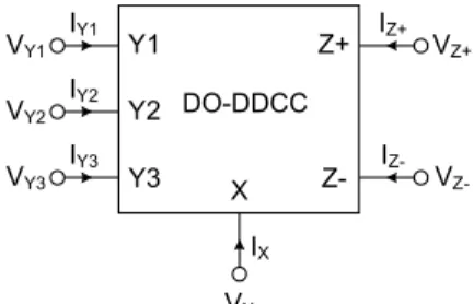
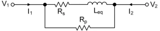
Lossy / lossless floating / grounded inductance simulation using one DDCC
Tam metin
Şekil
![Fig. 3. (a) Negative impedance converter given in [23], (b) its](https://thumb-eu.123doks.com/thumbv2/9libnet/4054370.57389/3.892.178.352.182.500/fig-negative-impedance-converter-given-b.webp)
Benzer Belgeler
The results for the inefficient institutional investors in the table indicate that the highest share of foreign investors is placed on the first quintile of beating performance..
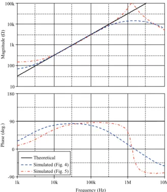
The gain responses of the fourth-order band-pass filter in Figure 12 are shown in Figure 13 where the first and second proposed FISs are separately employed.. The total
The value of the learning rate during the learning process was variable, but still less than 10 for most of the time as shown in the figure 4.8 After the end of
Structure Requirements (cont) • strength & stiffness – concerned with stability of
In order to improve diversity, if no improvement is achieved during the intra-route phase, the block insert phase and the block swap phase, the insert/split phase takes the
Color Doppler showing eccentric severe MR, C) Coronary angiography revealed single coronary ostium (left anterior oblique view), D) LMCA coursed down as LAD in the
Color Doppler showing eccentric severe MR, C) Coronary angiography revealed single coronary ostium (left anterior oblique view), D) LMCA coursed down as LAD in the
By adding additional values to the existing system our proposed system works by using the methodology of collaborative based filtering, content based filtering and hybrid
