Grating Coupler Integrated Photodiodes for Plasmon
Resonance Based Sensing in Fluidic Systems
Burak Turker[*a,b,c], Hasan Guner[*a], Sencer Ayas[a], Okan O. Ekiz[a], Handan Acar[a], Mustafa O. Guler[a]
and Aykutlu Dâna[a]
a UNAM, Institute of Materials Science and Nanotechnology, Bilkent University, Ankara, 06800, Turkey. b Department of Biomedical Engineering, Afyon Kocatepe University, Afyon, 03200, Turkey.
c Department of Electronics and Communication Engineering, Yıldız Technical University, Istanbul, 34349, Turkey.
*Authors e-mail addresses: [email protected] and [email protected]
Abstract: We demonstrate an integrated sensor combining a grating-coupled plasmon resonance
surface with a planar photodiode. Plasmon enhanced transmission is employed as a sensitive refractive index (RI) sensing mechanism and monitored via the integrated photodiode.
OCIS codes: (130.6010) Sensors; (240.6680) Surface Plasmons
1. Introduction
Surface plasmon resonance (SPR) sensors employed as sensitive refractive index (RI) sensing mechanisms represent one of the fastest developing label-free biosensor technologies with a vast variety of applications in biology, food safety, medical diagnostics, agricultural and environmental monitoring [1]. However, today the main concern in the development of SPR is geared toward the design of easy-to-fabricate, low-cost, compact and sensitive biosensors.
SPR sensors mainly differ in the optical platforms they are based on. Prism couplers [2,3], though result in comparable higher sensitivity values [4], their bulky nature makes it unsuitable for applications in integrated devices. Waveguide couplers [5] employing fibers, though appear to present the highest degree of miniaturization of SPR sensors, require expensive higher index prisms for the resonant coupling between a surface plasmon and a waveguide mode and moreover have to suffer from instable sensitivity responses due to deformations of the fiber. Due to their compact size, planarity and stability, gratings as plasmon couplers [6] are superior to prism and waveguide couplers.
2. Experimental
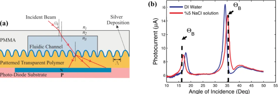
In this work we focused on eliminating one of the main integrity constraints of the design of compact SPR sensors and we replaced the traditional far field detecting (CCD/CMOS detector arrays) mechanism [7,8] used for detecting surface plasmons. The sensor assembly, schematically illustrated in fig. 1(a), has a sandwich structure of three integrated layers. On top, there exists a polymethyl methacrylate (PMMA) cover forming the flow channel. A photodiode substructure lying at the bottom serves as a detector and in between there is the patterned and metallised transparent polymer, i.e. the grating structure, to function as the surface plasmon (SP) coupler.
In order to demonstrate that the device can be realized on standard silicon substrates with low-cost and widely available manufacturing equipment, the photodiode was fabricated using a metal induced crystallization procedure
Fig. 1. (a) Cross-sectional schematic view of the integrated sensor device with an optimized grating structure having a 35 nm groove depth and 45 nm silver deposition, (b) Measured photocurrent response of the integrated sensor as a function
of the angle of incidence for water and NaCl solution. Bias angles used in the time-resolved measurements are shown by arrows. Wavelength of the incident light is 632.8 nm.
PMMA
Fluidic Channel Patterned Transparent Polymer Photo-Diode Substrate NP Incident Beam L Qi n 1 Silver Deposition n2 n3 (b)(a) (b) OSA/ CLEO 2011
CMX4.pdf
(b) (c) 30 32 34 36 38 0.05 0.1 0.15 0.2 0.25 0.3 0.35
Angle of Incidence, Degrees
Transmission
Bias Angle, Θi ΘR ΘR+∆ΘR
∆T
(a)
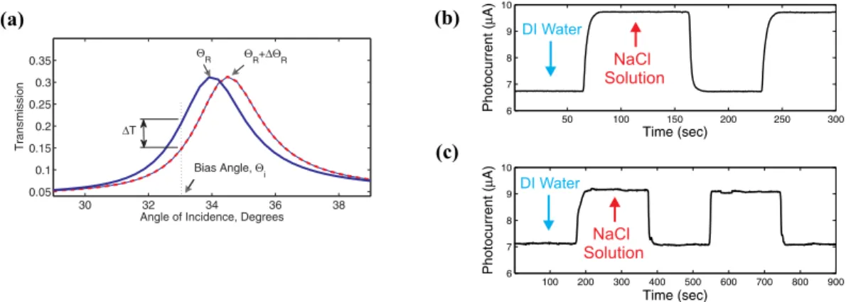
Fig. 2. (a) The operational principle of the device is schematically shown. The illumination is kept at a fixed angle Θi
and a small perturbation (∆ΘR) of the resonance condition (ΘR) results in a change (∆T) in the transmitted intensity.
(b) Sensor response to fluid exposures around the 2nd order resonance peak biased at 17.1˚ and (c) Sensor response to
fluid exposures around 1st order resonance peak biased at 35.6˚. A 632.8 nm HeNe laser source is used.
as described previously in ref. 9. Gratings were replicated using the elastomeric molding technique by
nano-imprinting [10,11]. Previously, we have shown that modified optical disc surface profiles can be used to excite sharp and well defined plasmon resonances [12]. Various tuned grating profiles were studied experimentally and
theoretically (using rigorous coupled wave analysis, RCWA[13]). Grating surfaces were characterized by using atomic force microscopy (AFM) and the plasmonic properties of silver coated gratings were characterized by measuring the reflection spectra using variable angle spectroscopic ellipsometry.
3. Results
We then integrated a microfluidic chamber and at the tuned AOI of a collimated external light source where the sharp plasmon resonance condition is enabled, we evaluated the readouts from the integrated photodiode which is monitoring the enhanced transmission of light and detecting the small RI changes (fig.1(b)) caused by the varying concentrations of alternating solutions. We experimented simply with DI (nominal refractive index 1.33) and 5% NaCl solution (nominal refractive index 1.342) and observed the shifts in the sharp plasmon resonance peaks. Following the operational principle described in fig. 2(a) our real time recordings revealed the repeatability and stability of the proposed sensor mechanism by observing photocurrent readouts relevant to both the first and second order resonance peaks (fig. 2 (b,c)). Using a low-power He-Ne laser beam we finally obtained an equivalent RI noise of 6.3x10⁻⁶
Hz
RIU / (limited by the laser intensity noise and instrumental drifts), compared to a shot-noise
limited theoretical sensitivity of 5.61x10⁻⁹ Hz RIU / .
4. References
[1] Hoa X. D. et al. “Towards integrated and sensitive SPR biosensors: a review of recent progress”, Biosens. and Bioelect. 23, 151–160 (2007). [2] Otto, “Excitation of nonradiative surface plasma waves in silver by the method of frustrated total reflection ”, Z. Phys. 216, 398 (1968). [3] Kretschmann, “The determination of the optical constants of metals by excitation of surface plasmons”, Z. Phys. 241, 313 (1971). [4] Homola, J., “SPR Sensors for Detection of Chemical and Biological Species”, Chemical Reviews 108 (2), 462-493, (2008). [5] Van Gent J. et al., “Optimization of a chemo-optical surface Plasmon resonance based sensor”, Appl. Opt., 29, 2843 (1990). [6] Dakss M.L. et al., “Grating coupler for efficient excitation of optical guided waves in thin films”, Appl. Phys. Lett. 16, 523, (1970). [7] Piliarik M., Vala M., Tichy I., Homola J., “Compact and low-cost biosensor based on novel approach to spectroscopy of surface plasmons”, Biosens. and Bioelect. 24, 3430–3435 (2009).
[8] Ouellet E. et al., “Parallel microfluidic surface plasmon resonance imaging arrays”, Lab Chip, 10, 581–588 (2010).
[9] Okan Oner Ekiz, Koray Mizrak and Aykutlu Dâna, “Chemically Specific Dynamic Characterization of Photovoltaic and Photoconductivity Effects of Surface Nanostructures”, ACS Nano, 4 (4), 1851-1860 (2010).
[10] Kocabas A., Dana A., Aydinli A., “Excitation of a surface plasmon with an elastomeric grating”, Appl. Phys. Lett. 89, 041123 (2006). [11] Kocabas A., Ay F., Dana A., Aydinli A., “An elastomeric grating coupler”, J. Opt. A: Pure Appl. Opt. 8, 85–87 (2006).
[12] Kaplan B., Guner H., Senlik O., Gurel K., Bayindir M., Dana A., “Tuning optical discs for plasmonic applications”, Plasmonics, DOI 10.1007/s11468-009-9099-x, (2009).
[13] International Intellectual Group, Inc., PCGrate. http://www.pcgrate.com.
[14] Gurel K., Kaplan B., Guner H., Bayindir M., Dana A., “Resonant transmission of light through surface plasmon structures”, Appl. Phys. Lett. 94, 233102 (2009).
OSA/ CLEO 2011