MULTIMODE MICROWAVE SENSORS FOR
MICRODROPLET AND SINGLE-CELL
DETECTION
a thesis submitted to
the graduate school of engineering and science
of bilkent university
in partial fulfillment of the requirements for
the degree of
master of science
in
mechanical engineering
By
Hande Aydo˘
gmu¸s
August 2018
Multimode Microwave Sensors for Microdroplet and Single-Cell Detec-tion
By Hande Aydo˘gmu¸s August 2018
We certify that we have read this thesis and that in our opinion it is fully adequate, in scope and in quality, as a thesis for the degree of Master of Science.
Mehmet Selim Hanay(Advisor)
Sel¸cuk Yerci
Emine Yegˆan Erdem
Approved for the Graduate School of Engineering and Science:
Ezhan Kara¸san
ABSTRACT
MULTIMODE MICROWAVE SENSORS FOR
MICRODROPLET AND SINGLE-CELL DETECTION
Hande Aydo˘gmu¸s
M.S. in Mechanical Engineering Advisor: Mehmet Selim Hanay
August 2018
A novel detection mechanism which can reveal both morphological and electri-cal properties of analytes are needed for Lab-on-a-Chip applications. Herein, a label-free, real-time and non-contact detection paradigm in microwave domain is constructed, by using first and second electromagnetic modes of a microwave resonator. As the resonator, microstrip line is chosen since it offers accessible boundary conditions. In order to deliver the analytes into the sensing region, mi-crofluidic channels are fabricated. As a proof-of-concept, while the microstrip line resonator’s first and second modes are tracked simultaneously, analytes are de-livered through the microchannel embedded underneath the signal layer. As the analytes, water microdroplets in oil, cervical (HeLa) and breast (MDA-MB-157) cancer cells in their appropriate medium are used and detected; their position and electrical volume informations are obtained and compared. Allan Deviation of the measurement is smaller than 2 × 10⁻⁸ for both modes, and due to analyte properties in microwave domain, such as the great permittivity difference between the biological analyte and medium, detection is possible.
In order to test the accuracy of finding the position of the analyte, two different microchannel geometries are designed. The first geometry is based on a zigzag channel, where microstrip line crosses the channel at 6 different locations. Sec-ondly, a branched channel is designed, to send the microdroplets at four different locations. This delivery mechanism is mostly based on the hydraulic resistance: Each droplet chooses its path by the hydraulic resistance that is caused by the previous droplet. Hence, microdroplets are distributed to four channels. Due to the mode shape of the specific mode, when analyte passing through these regions, it induces different frequency shifts. For these applications, microfluidic part is fabricated by conventional soft lithography methods, and the material for the microchannels is PDMS. Electrical volume of the droplets is also obtained.
iv
After the usage of prototypes for position and electrical volume calculations, second generation devices are fabricated. Compared to the PDMS-based devices, these devices offer rapid and low-cost prototyping. Additionally, Kapton is chosen for the dielectric material, and it has some material-wise benefits, such as the tangent loss level. Analytes are delivered through the sensing region by capillary tubings, hence soft lithography steps can be eliminated. Due to the equipment limitations, only the first mode is tracked with these novel devices, while another type of breast cancer cells (SK-BR-3) are delivered through the sensing region. Signal-to-noise ratio, when compared to the PDMS based devices, is improved.
In this work, the first two modes of microstrip line resonators are used. How-ever, by using higher order modes, more properties about the particles as skew-ness, geometrical volume, orientation, and composition can be obtained. These informations can be used to construct a global image of the analyte; rather than a pixel by pixel image. Additionally, flow cytometry applications, detection of Circulating Tumour Cells and applications for long term cultivation on chip (also known as Organ-on-Chip platforms) can be achieved.
Keywords: Microwave Resonators, Microfluidics, Lab-on-a-Chip Applications, Biosensors, Multimode Detection.
¨
OZET
C
¸ OK MODLU M˙IKRODALGA SENS ¨
ORLER˙I ˙ILE
M˙IKRODAMLACIK VE TEK H ¨
UCRE SAPTANMASI
Hande Aydo˘gmu¸s
Makine M¨uhendisli˘gi, Y¨uksek Lisans Tez Danı¸smanı: Mehmet Selim Hanay
A˘gustos 2018
Par¸cacıkların morfolojik ve electriksel ¨ozelliklerini tespit edebilen yeni sistem-ler, C¸ ip ¨Ust¨u Laboratuvar Uygulamaları i¸cin gereklidir. Bu ¸calı¸smada, mikro-dalga alanında, ger¸cek zamanlı, temassız ve etkitetleme ihtiyacı do˘gurmayan bir tespit etme yakla¸sımı; bir mikrodalga rezonat¨or¨un¨un ilk ve ikinci elektro-manyetik modları, kullanılmı¸stır. Sınır ¸sartları dolayısıyla, mikro¸serit hatlı bir rez¨onat¨or se¸cilmi¸stir. Par¸cacıkları algılama b¨olgesine ula¸stırmak i¸cin mikrokanal-lar ¨uretilmi¸stir. Kavramı kanıtlamak i¸cin rez¨onat¨or¨un ilk ve ikinci modu aynı anda s¨ur¨ul¨urken, par¸cacıklar, sinyal hattının altındaki bu mikrokanalları kulla-narak algılama b¨olgesine g¨onderilmi¸stir. Par¸cacık olarak ya˘g i¸cinde su mikro-damlacıkları; uygun besiyeri i¸cindeki rahima˘gzı (HeLa) ve meme kanser h¨ucreleri (MDA-MB-157) kullanılmı¸s ve saptanmı¸stır; bu par¸cacıkların pozisyon ve elek-triksel hacim ¨ozellikleri elde edilmi¸stir ve kar¸sıla¸stırılmı¸stır. Allan Sapması de˘geri iki mod i¸cin de 2 × 10⁻⁸ de˘gerinden az olup, mikrodalga rejiminde madde ¨ozellikleri dolayısıyla; ¨orne˘gin biyolojik par¸cacık ve par¸cacı˘ga ¨ozel be-siyeri arasındaki b¨uy¨uk elektriksel ge¸cirgenlik farkı, tespit etme mekanizmasını m¨umk¨un kılmı¸stır.
Sistemin pozisyon bulma algoritmasındaki do˘grulu˘gunu test etmek i¸cin, iki farklı mikrokanal geometrisi dizayn edilmi¸stir. ˙Ilk geometri, zigzag ¸seklindedir ve sinyal hattı ile altı farklı lokasyonda kar¸sıla¸smaktadır. ˙Ikinci geometri ise d¨ort kola ayrılmaktadır ve mikrodamlacıkları d¨ort farklı lokasyona g¨ondermek i¸cin tasar-lanmı¸stır. Bu g¨onderme mekanizması hidrolik diren¸c mekanizmasını temel alarak ¸calı¸sır: Her damlacık gidece˘gi kanalı ondan bir ¨once giden kanalın yarattı˘gı hidro-lik dirence g¨ore belirler, b¨oylelikle d¨ort kanala da damlacık da˘gılımı g¨ozlemlenmi¸s olur. Par¸cacık sinal b¨olgelerinden ge¸cerken g¨oz ¨on¨unde bulundurulan her modda farklı bir frekans kaymasına sebep olur. Bunun sebebi de her modun, ayrı bir
vi
mod ¸seklinin olmasıdır. Bu uygulamalardaki mikrokanal kısmı mikroakı¸skanlarda yaygın kullanılan litografi metodu ile ¨uretilmi¸stir ve mikrokanalların ¨uretiminde PDMS maddesi kullanılmı¸stır. Mikrodamlacıkların elektriksel hacmi de hesa-planmı¸stır.
Prototip aletler pozisyon ve elektriksel hacim hesaplamalarında kullanıldıktan sonra, farklı cihazlar da dizayn edilmi¸s ve ¨uretilmi¸stir. Bu yeni jenerasyon ciha-zların ilk modellerden en b¨uy¨uk farkı ise daha ucuza ve daha hızlı ¨uretilmeleridir. Ayrıca, dielektrik materyal olarak Kapton se¸cilmi¸stir ve Kapton’un kayıp tan-jantı de˘geri ba¸sta olmak ¨uzere bazı ¨ust¨un materyal ¨ozellikleri bulunmaktadır. Par¸cacıklar algılama b¨olgesine kapiler boru ile g¨onderilmi¸stir; b¨oylelikle litografi metodu ve di˘ger fabrikasyon y¨ontemlerine duyulan ihtiya¸c ortadan kaldırılmı¸stır. Kullanılan ekipmanların ¸calı¸sma limitlerinden dolayı, yeni nesil cihazlarda sadece ilk mod s¨ur¨ulm¨u¸st¨ur ve denemek i¸cin ba¸ska bir t¨ur meme kanseri h¨ucresi (SK-BR-3) saptanmı¸stır. ¨Onceki aletlerle kar¸sıla¸stırıldı˘gında, sinyal g¨ur¨ult¨u oranında bir iyile¸sme g¨ozlemlenmi¸stir.
Anlatılan ¸calı¸smada mikro¸serit hatlı rez¨onat¨or¨un ilk iki mod kullanılmı¸stır. Bununla birlikte, ¨ust seviye modlar kullanılarak par¸cacıklarla ilgili daha ¸cok bilgi; geometrik hacim, e˘grilik, oryantasyon, par¸cacı˘gın bile¸simi, elde edilebilir. Pikselli g¨or¨unt¨u alımındansa bu bilgiler ile par¸cacı˘gın global g¨or¨unt¨ulemesi elde edilebilir. Ek olarak bu sistem, akı¸slı h¨ucre sayımı aplikasyonlarında, dola¸sımdaki t¨um¨or h¨ucrelerinin saptanmasında ve uzun d¨onem ¸cip ¨ust¨u h¨ucre k¨ult¨urleme ara¸stırmalarında (bu platformlar C¸ ip-¨ust¨u-Organ olarak da bilinmektedir) kul-lanılabilir.
Anahtar s¨ozc¨ukler : Mikrodalga Rezonat¨orleri, Mikroakı¸skanlar, C¸ ip ¨Ust¨u Labo-ratuvar Uygulamaları, Biyosens¨orler, C¸ ok Modlu Algılama.
Acknowledgement
I sincerely want to thank my advisor, Dr. Selim Hanay, who taught me the meaning of interdisciplinary science. Without Dr. Hanay, I would not be this scientist who has a mechanical engineering degree, and working with cancer cells and I cannot thank enough for his support, knowledge, and guidance. I wouldn’t have learnt this much, if I was not working with you sir. I am thankful to my MS thesis committee, Dr. Yegˆan Erdem and Dr. Sel¸cuk Yerci for their valuable time.
Hanay Research Group; each of you taught me so many stuff -whether or not related to our research-, and it is a privilege to work with you. Ezgi Orhan, Levent Aslanba¸s, Arda Se¸cme, Utku Hatipo˘glu, thank you for your valuable contribu-tions, exchange of ideas. Sel¸cuk O˘guz Erbil, thank you for your close friendship and all the times we spent in the cleanroom, trying to fabricate the best chips. Mert Y¨uksel, thank you for your help, close and thoughtful friendship; and all the coffee we had. Mehmet Kelleci, I cannot thank you enough. Where should I begin? This work would not be where it is without you, and you taught me so much. You are the best ”lab-mate” anyone could have and it is an honour to be in the same project with you. You are more than a brother to me, and always the companion in misfortune. Finally, our alumni, C¸ a˘gatay Karakan and Atakan Bekir Arı, thank you for your guidance and friendship.
Irmak Ulusoy and Barı¸s Top¸cu, my dearest friends, thank you for your support, and being there for me, all the time. All the graduate students at the Department of Mechanical Engineering; Ozan Temiz, M¨uge ¨Ozcan, Cem Kurt, Dilara Uslu, Levent Dilavero˘glu, Hammam Mohamed; thank you all for the moral support, I hope which is mutual, it is a privilege to walk on the same road with you. Onur Vardar, thank you for being one of the closest friends, and valuable discussions.
I want to express my gratefulness to my family. My dad, Teo, a dedicated engineer who has influenced me the most in this path. Mum, there is not enough words to explain my love, my gratitude. I (hope to) believe I got your work ethics,
viii
thanks to the sleepless nights in the gynaecology clinic, when you were working for limitless hours. My sister, my best friend, Zeynep, literally I would not be this person without you. Even though we have moved to two different continents, I feel your unconditional love and support, on every subject. Without you guys, I would not be this scientist who is trying her best.
Finally, women in engineering and science, please do not hesitate to improve yourselves to become your better versions, always work hard, and believe in yourselves. “We can do it.”
Contents
1 Introduction 1
1.1 Microfluidics and Lab-on-a-Chip Devices . . . 2
1.2 Mechanical Domain . . . 5
1.2.1 Inertial Imaging . . . 5
1.2.2 Suspended Microchannel Resonators . . . 6
1.3 Analogy Between Mechanical and Microwave Domains . . . 7
1.4 Microwave Resonators Integrated with Microfluidics . . . 7
1.5 Thesis Outline . . . 9
2 Microwave Domain 11 2.1 Imaging in Microwave Domain . . . 11
2.1.1 Theory Behind Imaging . . . 13
2.1.2 Measurement Devices, Circuit and Two Mode Tracking . . 16
CONTENTS x
3.1 Sample Preparation . . . 19
3.2 Soft Lithography . . . 20
3.2.1 Mask Preparation . . . 21
3.2.2 Preparation of the Master . . . 21
3.2.3 PDMS Preparation . . . 25
3.2.4 Ground & Strip Layers . . . 26
4 Droplet Detection with Microstrip line Resonator 30 4.1 Droplet Microfluidics . . . 31
4.1.1 Capillary Number . . . 31
4.1.2 Flow Rate Ratio . . . 32
4.1.3 Geometry . . . 33
4.1.4 T-Junction for Droplet Formation . . . 33
4.2 Droplet Detection with a Zigzag Microchannel . . . 34
4.3 4-Branched Microchannels for Droplet Distribution, Location and Electric Volume Calculations . . . 36
5 Cancer Cell Detection & Differentiation 40 5.1 Cell Detection . . . 43
5.1.1 Electrical Volume Difference . . . 45
CONTENTS xi
6 Novel Facile Resonators 49
6.1 Fabrication . . . 50 6.2 Cell Experiment . . . 51 6.3 Kapton Etch Trials . . . 52
7 Conclusion and Future Works 57
7.1 Organ-on-Chip Platforms . . . 58 7.2 Fused Silica Device Fabrication . . . 61
A Cell Culture 71
A.1 Cell Medium Composition . . . 71 A.2 Cell Culturing Equipments . . . 72
List of Figures
2.1 Schematic of microstrip line resonator with microchannel. First and second modes and mode shapes are indicated. . . 12 2.2 Schematic of the circuit which is used for simultaneous two modes
tracking of the microwave resonator. . . 17 2.3 Schematic of PLL circuit; measurement system for each mode.
Reprinted with permission of Royal Society of Chemistry, Lab on a Chip Journal, Issue 3, 2018. . . 18
3.1 Photomasks for microfluidic applications. . . 21 3.2 Schematic of photolithography onto negative photoresist. . . 23 3.3 Si wafer with SU-8 structures; in this case a 8-branched
microchan-nel. To use only 4-channels, a portion of SU-8 is removed from the mask. . . 25 3.4 Si wafer with SU-8 structure; namely a single microchannel
geom-etry. Width of the channel is approximately 50µm. . . 25 3.5 Silicon with SU-8 structures. A thin layer of PDMS is poured and
LIST OF FIGURES xiii
3.6 Final products for different applications. Coloured DI water is filled in order to embellish the microchannels. . . 27 3.7 Fabrication schematic of the device. . . 28 3.8 Final product for a device with a zigzag microchannel. . . 28 3.9 Port connector with epoxy. 4 branch of microchannels and
mi-crostrip are also visible. . . 29
4.1 T-Junction for droplet formation. Water droplets are formed with carrier fluid, oil. . . 34 4.2 Frequency shifts on first and second modes due to droplet passage.
Point E is approximately at the center of the device. . . 35 4.3 (a)4 microchannels that are used for droplet distribution.
(b)Histogram of 121 droplets and their choice of microchannels. (c)Frequency shifts on both modes, due to droplet passage from one of the channels, A to D. . . 37 4.4 Droplet sorting by branching the microchannels. Two droplets
are visible. Second droplet favours channel with lower hydraulic resistance. . . 38 4.5 Position data of the droplets in frequency shift domain. Inset also
shows how position and electrical volume contours are calculated. Reprinted with permission of Royal Society of Chemistry, Lab on a Chip Journal, Issue 3, 2018. . . 38 4.6 Droplet information. Reprinted with permission of Royal Society
LIST OF FIGURES xiv
5.1 HeLa cells’ histogram. Inset image shows microscopy image of
HeLa cells. . . 41
5.2 MDA-MB-157 cells’ histogram. Inset image shows microscopy im-age of the same cells. . . 41
5.3 Control runs for Allan Deviation calculations. Response time of both modes can be observed. Reprinted with permission of Royal Society of Chemistry, Lab on a Chip Journal, Issue 3, 2018. . . 43
5.4 Allan Deviation plots for the first and second modes. . . 44
5.5 Frequency shifts on both modes due to HeLa passage. . . 44
5.6 Frequency shifts on both modes due to MDA cells’ passage. . . 45
5.7 Frequency shifts on both modes due to a group of HeLa cells. . . 45
5.8 Electrical volume histogram of HeLa cells and microdoplets. Out-liers indicate entry of multiple cells into the channel at the same time. The inset compares the size of the HeLa cells to the size of the microdroplets. . . 46
5.9 Electrical volume comparison of the HeLa and MDA-MB-157 cell lines. Reprinted with permission of Royal Society of Chemistry, Lab on a Chip Journal, Issue 3, 2018. . . 46
5.10 Optical microscopy images of breast cancer cells. . . 47
5.11 Size comparison of wild type and treated breast cancer cells. Since they are similar in size, it is difficult to compare their electrical volume. . . 48
LIST OF FIGURES xv
6.2 Frequency shifts on first mode due to single cell passage events. . 51 6.3 Allan Deviation of the first mode. . . 52 6.4 First mode frequency shift histogram. . . 52 6.5 Optical microscopy images of etching where SU-8 is used as the
masking material. . . 54 6.6 SEM image of etching from different perspectives. . . 54 6.7 SEM images of etching when the chrome is used as the masking
material. . . 56
7.1 Microscope inside an incubator, surrounded by faraday cage. . . . 61 7.2 Schematic of fused silica sample after inlet-outlet openings and
lithography. . . 62 7.3 Schematic of the sample with ground layer and microchannel. . . 63
B.1 Droplet formation trial while Vwater is greater than Voil. . . 74
B.2 Droplet formation trial while Vwater is smaller than Voil. . . 74
List of Tables
3.1 Spin Coating Parameters for 200µm Resist . . . 22
3.2 Spin Coating Parameters for 75µm Resist . . . 22
3.3 Photolithography Parameters . . . 24
3.4 Photolithography Parameters for 75µm thickness of SU-8 . . . 24
4.1 Flow Rates of the Continuous and Dispersed Flows . . . 33
4.2 Normalized Positions of the Microchannel Sections Where They Cross the Signal Line. . . 35
Chapter 1
Introduction
This thesis introduces a novel detection mechanism in microwave domain, which is integrated with microfluidics. As a laboratory whose work is mostly in mechanical domain and Nanoelectromechanical Sytems and their vibrational modes, moving to microwave domain was not a burden due to the analogy between mechanical and microwave domains. In this work, a microstrip line resonator is fabricated with a microfluidic channel embedded between its signal and ground layers. In theory, while the microwave resonator’s higher order electromagnetic modes are tracked simultaneously, and if an analyte is delivered to the sensing region, mor-phological and electrical properties of this analyte can be extrapolated. These kind of Lab-on-a-Chip devices are needed especialy for biological experiments, since biological analytes which are needed to be sensed should be in appropriate medium, in order to maintain their viability. For this work, first two electromag-netic modes are tracked, and position and electrical volume of the analyte are gathered. As a proof-of-concept, first experimental trials are done with water mi-crodroplets in oil. Due to permittivity difference, simultaneous frequency shifts on both modes are observed. In order to study position calculations, different mi-crochannel structures are designed and fabricated. Secondly, HeLa (cervical) and MDA-MB-157 (breast) cancer cells are tracked. Each single cell causes frequency shifts on all considered modes. Their electrical volumes are also differentiated. Even though there is a great volume difference (orderwise) between the resonator
itself and the analyte which is desired to be sensed, namely cancer cells; Allan Deviation results which are lower than 2 × 10⁻⁸ and microwave frequency range make sensing possible.
First prototype resonators’ microfluidic parts are based on PDMS and soft-lithography techniques. Another prototype is also developed, which is based on capillary tubings. This new type of devices are low-cost, and can be rapidly produced. With this detection mechanism, label-free and real-time detection of biological analytes, namely cancer cells can be achieved.
With multi-mode sensing techniques, rather then pixel by pixel imaging, global image of the analyte can be constructed. This label-free and real-time sensing platform offers characterization of cells, and in the future, it can be used for flow cytometry applications, analysing the composition of biological particles, or detection of Circulating Tumour Cells.
1.1
Microfluidics and Lab-on-a-Chip Devices
Fabrication of microsystems began as early as in the late 1960s, with advance-ment in nano-micro fabrication techniques. Microfluidic technologies, with vari-ous advantages, as using small volumes of samples, short times of analysis, low cost, carrying out chemical reactions with high resolution and sensitivities[1], and capability of integrating different life sciences, evolved from microsystems. Microfluidics involved in different branches. First applications of microfluidics include chromatography platforms. In 1990s, defense industries aimed to deploy microfluidics for chemical and biological threat detectors in warzones. Another application was the first trial of the ink-jet printing technology[2]. Addition-ally, biological applications as DNA sequencers[3] had been introduced, as rapid platforms compared to their macro-sized counterparts.
With the advancement in microfluidic technologies, researchers have started to integrate systems in one chip. Depending on the application, this chip includes
microchannels, electronic parts for transduction and read-out, mixers, pumps, valves. Hence, it abolishes the need for major equipments, and the chip itself gathers laboratory techniques into a system. This is how microfluidics evolved to lab-on-a-chip; not just the microchannels, but necessary systems to extract data for various applications are included in this major field. Of course, researchers should have a focus on some requirements when developing a new LoC system, as being sensitive, low cost, compact, and the test that take shorter time to result then macro counterparts[4].
Moving from macro to micro scale has specific advantages. One of the main advantage is that capillary forces become more dominant, and passive fluidic ac-tuation becomes favourable[5]. Reynolds Number, a dimensionless number which is the ratio of inertia force to viscous force, therefore which specifies the flow regime, can be used to characterize whether the flow is in the laminar or turbu-lent regime.
Re = ρuL
η (1.1)
Where ρ is the density of the fluid, u is the velocity of the fluid, L is the characteristic length, and η is the dynamic viscosity of the fluid. In microfluidics, due to its dimensions, flow is usually described with small Re; therefore in lam-inar regime. If Navier-Stokes equation is also investigated in micro domain for newtonian and incompressible fluid flow:
ρ(∂(u)
∂t + u.∇u) = −∇p + η∇
2
u (1.2)
Which can be interpreted as acceleration terms versus the force terms. The first term implies the acceleration due to unsteadiness, second term is the convective acceleration of the velocity field, third term is the pressure gradient, and final term is the viscous force. At micro scale, assuming unidirectional steady fluid flow, the equation becomes Stoke’s equation:
∇p = η∇2u (1.3)
changes in the flow. Laminar flow also shows some characteristics as being lin-ear, reversible, steady and independence from inertia. Hence, microfluidics have unique properties, which result in well-defined and stable liquid-liquid interfaces, due to smaller dimensions. Thus, even at single cell level effects can be examined [5].
As it is mentioned above, cell studies gain importance with LoC devices. How cells behave inside human body is the main question for Point of Care appli-cations. These applications try to investigate different drug delivery systems, diagnosis, and how every individual responses to different types of drugs. The main goal is to develop a portable low-cost instrument, a real Lab on a Chip, in order to get rid of expensive lab equipments, and to especially reach to people in rural settlements. An example for a point of care device is the cell counting and sorting platform, a flow cytometer, which consists of a disposable microfluidic chip, and a miniaturized detection system [6].
For biological studies, cell to cell as well as cell to extracellular matrix interac-tions have being investigated. There are different research groups that examine cell growth rates by mimicing complex extracellular matrix [7], isolation of in-dividual cells by using microfluidic sorting devices with appropriate biological assays [8], or use impedance sensing with dielectrophoretic cages to manipulate microorganisms, without any chemical labeling [9].
As it can be examined, microfluidics and Lab-on-a-Chip devices have various applications, and in the beginning of 2000s, biomicrofluidics gained a different perspective, especially with the development of single cell sorting, monitoring, and manipulating platforms. After nearly 18 years, these devices still have great potential, yet to be discovered, to solve diagnostic problems, to gain a sight for various types of tumour cells.
In this work, microfluidics are used for droplet forming and sorting, and cell delivery to the sensing area. These parts will be discussed in detail, on the following sections.
Cells are cultured in petri dishes, and these dishes do not mimic their natural environment; human body. Organ-on-chips, namely cell culturing platforms that try to mimic a part of a tissue or an organ, by using microfluidics. These platforms are especially important to understand how a drug affects that specific cell group, and cells do react differently in situ. Organ on chips will also be covered in the Future Works Section, in order to investigate how our system can be integrated with these kind of platforms.
1.2
Mechanical Domain
In this section, mechanical domain refers to the vibrational modes of resonators, Nano an micro electromechanical systems, and how information about analytes can be extracted by using these platforms.
1.2.1
Inertial Imaging
Nano and micro resonators are used for weighing analytes of different size and composition ranging from gold nanoparticles to bacteria and they may be used to detect biological analytes such as live cells [10].
When an analyte lands on a nanomechanical resonator, for instance on a double-clamped beam, it will induce frequency shifts, depending on the mass and position of the analyte, on each corresponded mechanical modes.
By using multiple vibrational modes of a resonator, spatial information of analytes as mass, shape and size can be obtained, in real-time. After obtaining these spatial properties, an image can be constructed. This reverse imaging algorithm is known as Inertial Imaging [11]. Since fluctuations of the frequency response give the resolution, ultrasensitive measurements are achievable.
1.2.2
Suspended Microchannel Resonators
As it is explained, nano and micro resonators can be used to obtain spatial proper-ties of biological analytes. It is desirable to examine the characteristics of biolog-ical particles as cells in a suitable solution, to maintain their viability. However, when resonators are surrounded with fluid, viscous damping of the fluid degrades quality factor, resulting in low sensitivity.
In 2003, a research group from MIT came out with the idea of Suspended Mi-crochannel Resonators, SMR, in which the fluid channel is inside the resonator, kept at vacuum. SMR are excited on their higher modes, simultaneously, to extract information about particles. They eliminated viscous damping effects, hence obtained high quality factors and high sensitivity [12]. The first exper-iments were detection of the binding of avidin and biotinylated bovine serum albumin, in real-time. They continued with measuring individual particle masses with femtogram resolution [13], weighing bacterial cells, with high quality factor (15,000) resonators, without binding [10], density characterization of human red blood cells and E.Coli [14], density differentiation of two different cancer cell lines by using dual-SMR[15].
Apart from single cell studies, cell growth rates are also being studied. These studies have major impact, since they are directly related to drug susceptibility testing, as it is explained at Microfluidics and Lab-on-a-Chip Devices Section. They are weighing cells; namely mouse and human T cells, repeatedly while flowing cells from the microfluidic channel with several resonant mass sensors. They obtain cellular responses of cells to antibiotics [16]. At another study, they are measuring the mass accumulation rate of tumour cells, MAR, in order to investigate the drug sensitivity for every individual patient, and single cell therapeutic responses [17]. Drug sensitivity of single multiple myeloma cells are also examined by using MAR. Due to the high rates of drug resistance, finding the most effective theraphy is needed [18].
As it can be examined, micro and nano resonators have being used widely, for various applications. However, there are some drawbacks. Especially, the
fabrication of Suspended Microchannel Resonators is challenging; etching mi-crofluidic channels on silicon, or anodic bonding to enclose them. Moving from mechanical domain to electromagnetic domain can expedite the fabrication pro-cess. Additionally there are similarities between these two domains, and they will be investigated at the next section.
1.3
Analogy
Between
Mechanical
and
Mi-crowave Domains
Inertial Imaging principles, developed for NEMS, can be extended to electromag-netic resonators as well. Higher-order modes of microwave sensors have not being used for extracting morphological properties. However, in mechanical domain, micro and nanomechanical sensors have been driven in their higher-order modes to obtain information as measuring mass and stiffness of particles [19], weighing particles in real time [11], and getting spatial properties to form inertial imaging of the particle [20], as stated above.
While an analyte travels through the sensing region, it causes frequency shifts in all considered modes, similar to mechanical domain. These frequency shifts depend on the analyte, and the mode shape. When the frequency shifts from all modes considered, global properties of the analyte can be extracted. These features can be electrical volume, position, and shape of the analyte. Hence, global image of an analyte can be extracted.
1.4
Microwave Resonators Integrated with
Mi-crofluidics
Microwave resonators have being used with fluidics for different applications. One of the early applications is the characterization of different liquids by comparing
dielectric properties by using coplanar sensors[21]. However, this integration is not with in micro-scale, but with greater volume of liquids. Similar application with smaller volumes of liquid, on the order of nanoliter, has been investigated after almost a decade from aforementioned work [22]. Some of the microwave resonators for dielectric property characterization of liquids do not need expen-sive equipment for fabrication; instead, resonator can be integrated with capilary tubings [23]. Additionally, concentration characterization can be achieved, and researchers have investigated the glucose concentration in water, by measuring the resonance property of the resonator, with a microstrip line resonator [24]. Es-pecially with the technological improvement of micro-nano fabrication techniques, biological applications, bio-sensors, gain a momentum as well. By using a HF-based sensing technique, a coplanar waveguide platform, researchers have shown label-free, contactless detection for biological analytes, namely human umbilical vein endothelial cells, by using micro-liter volumes of liquid [25].
In order to develop an electronic sensing platform for biological analytes, ions in cell medium should be taking into consideration, since they will compose electri-cal double layer [26]. This double layer causes sensing problems at low frequency domain; however, at microwave band, electromagnetic sensing is not limited by Debye screening [27]. Therefore, microwave sensors, resonators, can be used as a label-free biosensing platform for biological analytes, and morover single cell detection can be achieved. Researchers have shown that baker’s yeast (Saccha-romyces cerevisiae) and Chinese hamster ovary cells can be detected in suspend-ing fluids as phosphate-buffer saline by microwave resonator integrated with an interferometer [28].
In the works that are mentioned above, generally network analyzers are used. Network analyzers are used to test designs which are in the RF or microwave regime by measuring their response. In our work, network analyzer is only used to characterize the initial values. First two modes of the resonator are tracked by a system that is designed for real-time and sensitive measurement.
1.5
Thesis Outline
Chapter 1 gives information about microfluidics and Lab-on-a-Chip platforms, sensing in mechanical domain; namely mass spectrometry, inertial imaging. It moves on to suspended microchannel resonators, devices with embedded microflu-idic channels to obtain mass, size, density information about biological analytes, without getting affected by viscous damping of the fluid which carries these an-alytes. These resonators are excited in their vibrational modes, and despite the fact that they have various applications and high sensitivity levels, fabrication of such devices is a drawback. This chapter continues with the analogy between mechanical and microwave domains, and concludes with some examples in the literature which use microwave resonators integrated with microfluidics.
In Chapter 2, microwave imaging is introduced. This novel platform is a varia-tion of inertial imaging from mechanical domain, in order to obtain morphological and electrical properties of analytes.
In Chapter 3, fabrication of microstrip line resonators integrated with microflu-idics is explained. Fabrication has various steps, both in the cleanroom and in the lab environment. Basically, it is a combination of soft lithography and device bonding.
In Chapter 4, droplet microfluidics and how it is implemented to microwave imaging is investigated. Two different types of microchannels are fabricated; zigzag and 4-branched. Zigzag microchannel is used to detect water microdroplets in oil, and branched microchannel is used to characterize droplets’ position and electrical volume, while they are passing through the sensing region.
In Chapter 5, different cancer lines, cervical (HeLa) and breast (MDA-MB-157) are used for microwave imaging. Detection of cells and electrical volume differentiation is presented.
In Chapter 6, novel microstrip line resonators are introduced. These devices are based on Kapton, and do not need any cleanroom process or equipment.
They are low-cost, easy and fast to produce. Experiments are done with SK-BR-3 breast cancer cells, with the first mode of the resonator.
In the final chapter, conclusion of the work is presented and future works are discussed. These platforms can be integrated with Organ-on-Chips to further investigate drug susceptibility, resistance or to study cell-to-cell interactions.
Chapter 2
Microwave Domain
In this work, resonators which work in microwave regime are used. Microwave band is named for electromagnetic waves between 1GHz to 300GHz frequencies. The reason to use these type of resonators is due to the fact that these type of short wavelengths offer some advantages, and these advantages are explained in this section.
Microwaves radiate electromagnetic energy, travel in straight lines, and they are reflected by conducting surfaces. Waves propagate through transmission lines, by transmitting energy. Basically, transmission lines can be divided into two groups: Multiconductor Lines and Waveguides; which are Single Conductor Lines. There are some differences between multiconductor lines and waveguides, as supporting TEM wave, having a cut-off frequency or not, amount of reflections, dispersion of waves and limitations on bandwidth. In the works presented here, microstrip line resonators, which are in the multiconductor lines group, are used.
2.1
Imaging in Microwave Domain
New detection techniques in microwave regime offer some potential by being com-pact, low-cost, and sensitive. These electronic sensing techniques are integrable,
and in this work, microstrip line resonators integrated with microfluidics are used to obtain morphological and electrical properties of anayltes; namely water micro-droplets in continuous oil, and various cancer cells in their appropriate medium. Morphological properties such as position and shape of an analyte can be ex-tracted by using higher-order modes of the sensor. Once these informations are available, global image of the analyte can be constructed.
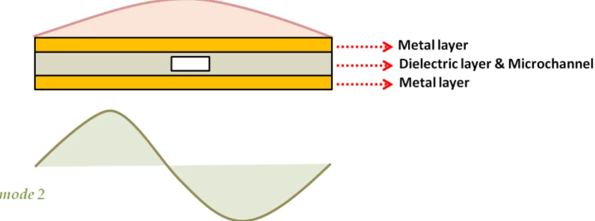
Figure 2.1: Schematic of microstrip line resonator with microchannel. First and second modes and mode shapes are indicated.
As it is explained at Chapter 1, integration of microwave resonators with mi-crofluidics, microwave regime has some unique properties. One of them is the fact that Debye screening is not a limitation, as in the case of low frequency applications.
Permittivity of materials depend on temperature and frequency. For instance, water has a permittivity around 80 below 3GHz, and it decreases with increasing frequency [29].If biological analytes is taken into account, as proteins (4-6, below 3GHz), one can observe the contrast between relative permittivity values at the microwave regime [30]. To give different information about biological tissues, one can examine [31] and [32]. One thing in common is the relative permittivity values for these tissues, ranging from bone to kidney, are around 10. Hence, this contrast between biological particles and medium that carry them makes microwave imaging favourable, since at optical frequencies, refraction of biological materials and carrier fluids are similar.
2.1.1
Theory Behind Imaging
When there is a change in the permittivity of the dielectric material, in this case due to the passage of an analyte through microchannel embedded inside the mi-crostrip line resonator, it causes frequency shifts. These frequency shifts, denoted with ∆fn, are related to ε; dielectric constant of the medium, µ; permeability of
the medium, En and Hn are the electrical and magnetic field for the nth mode.
∆fn fn = − R V0∆ε(r)E 2 n(r)d3r R V0(ε(r)E 2 n+ µ(r)Hn2)d3r (2.1)
The equation can be simplified further by taking into consideration at reso-nance condition, since right hand side denominator is the total stored energy of the resonator: * Z εEn2d3r + = * Z µHn2d3r + (2.2)
After substituting harmonic oscillator property, the frequency shift equation becomes: δfn= − R V0∆ε(r)φ 2 n(r)d3r 2R V0ε(r)φ 2 nd3r (2.3)
Where the left side is the fractional frequency shift. The denominator can be thought as the effective electrical volume of the considered mode, Vn, and the
equation becomes: δfn= − R V0∆ε(r)φ 2 n(r)d3r 2Vn (2.4)
If the analyte is thought as a point particle, where its shape or size is arbitrary in the given context, dirac delta function can be taken into account. Therefore,
∆ε(r) becomes:
∆ε(r) = νδ(r − rp) (2.5)
Where ν is the excess electrical volume, and rp is the position of the point
particle. If the dielectric constant is replaced:
δfn= − νφ2 rp 2Vn = −νφ 2 x 2Vn (2.6)
As it is explained above, in this work microstrip line resonators are used. These resonators are one-dimensional, hence frequency shifts for the first two modes can be simplified into: δf1 = − νφ1(x)2 2V1 (2.7) δf2 = − νφ2(x)2 2V2 (2.8)
These two equations leave two unknowns, namely ν and φ.
As it can be examined from the equations above, frequency shifts are propor-tional to the square root of the electric field. Fringing fields can be neglected, since active region is directly under the microstrip line, at z direction. Thus local electric field equation can be written with amplitude An and mode shape, φn, in
the z direction.
En(r) = Anφn(x)˜k (2.9)
As it will be investigated further on the upcoming sections, microstrip lines used in this work are shorted from both ends, creating boundary conditions.
Hence the mode shape function can be expressed with φn = sin(nπx), and this
function can be replaced in the main equation. Hence the electrical volume of a particle can be calculated with:
δfn= −
ν sin2(nπx) 2Vn
(2.10)
To find the location of the particle, after excess electrical volume is known, deltaf1 and deltaf2 can be substituted. By using only half of the device:
δf2 δf1 = −sin 2(2πx) sin2(πx) (2.11) δf2 δf1 = −4 sin 2(πx) cos2(πx) sin2(πx) (2.12) δf2 δf1 = −4 cos2(πx) (2.13) Finally; x = 1 πarccos s δf2 δf1 ! (2.14)
In conclusion, by using the first two modes of the microstrip line resonator, an analyte passing through inside the microchannel, which is embedded inside the resonator, position and electrical volume calculations can be done.
To verify the experimental results of electrical volume and position, Maxwell-Garnett approach can be used. This approach allows to approximate effective permittivity, since it concerns the host medium, and replacement of this medium by another media. In the equation, εi is the permittivity of the disperse flow
(water for droplet experiments or cells for cancer cell detections), εh is the
detections), and f is the filling ratio, which explains the quantitative change of the disperse and continuous liquids.
∆ε = 3f εh
εi− εh
εi+ 2εh
(2.15)
2.1.2
Measurement Devices,
Circuit and Two Mode
Tracking
As it is explained in the Introduction Chapter, network analyzer is only used for the first characterization of the device. The first characterization includes finding modes of the resonator. For the microstrip line resonator integrated with a 4-branched microfluidic channel, first mode of the device is at 1.49GHz and second mode is at 2.97GHz, and quality factors are 54 and 48, respectively [30]. Quality factor is the ratio between stored energy over dissipated energy, and characterizes as the name implies, quality of the resonant platform.
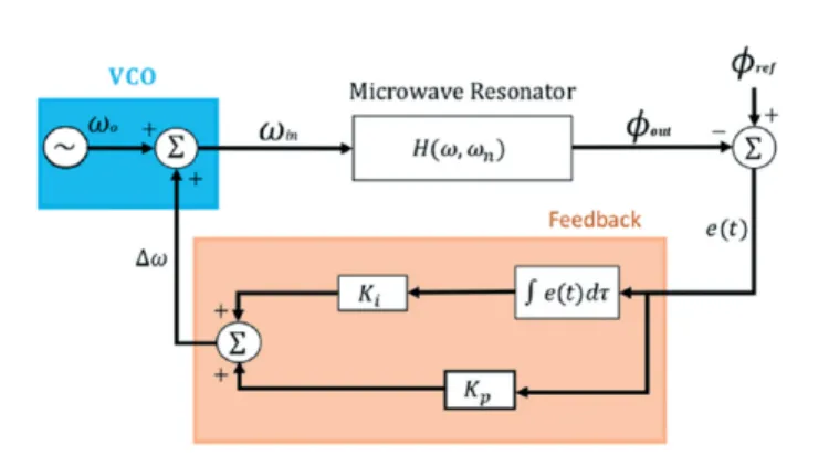
For the tracking of the resonance frequencies of the first and second modes in real-time, a system is constructed. This system is based on two digitally controlled signal generators and two lock-in amplifiers [30]. In the system, signal generator generates the electrical signal in the waveform, and lock-in amplifiers basically extract amplitude and phase of the signal, even in a noisy environment. The measurement setup consists of two parallel circuits with microwave com-ponents as Power Splitter, RF Switch, Power Combiner, and Mixer. The circuit itself can be examined at Figure 2.2. In this figure, ’w’ denotes the first mode fre-quency, and ’2w’ denotes the second mode frequency of the microwave resonator. Lock-in Amplifier frequencies are indicated to simplify the circuit; to make the task of the microwave components explicit. Power splitter takes one input sig-nal and dispatches multiple output sigsig-nals, which are isolated from each other, and have equal amplitudes. It can be used in reverse, to be Power Combiner. RF Switch is used to obtain the modulated ∆w frequency, which is taken from Lock-in Amplifier, in TTL signal form. Mixers basically multiply two signals, a
Figure 2.2: Schematic of the circuit which is used for simultaneous two modes tracking of the microwave resonator.
non-linear process, and are important at signal processing. It can be taught as the outcome of the mixer will be signals with different frequencies. Finally, a low pass filter, or a band-pass filter, (according to the lock-in amplifier frequency), can be used just before the lock-in amplifier input, to make the signal less noisy. At resonance frequencies, the phase of the resonator is locked at 0°. Deviation from 0° (for example, due to the passage of an analyte from the microfluidic channel embedded inside the microwave resonator) creates an error signal. This error signal is used the update the frequency, and the update mechanism is based on a PI-Controller (Proportional-Integral Controller).
u = Kpe + KI
Z
edζ (2.16)
In the setup, two parallel phase-locked loop(PLL) systems are used. It is basically an update mechanism with a feedback loop. In this work, at Chapter 4, (where water microdroplet passages create error signal) and Chapter 5, (where
single cell passages create error signal), experiments that use this measurement setup are explained. In summary, VCO routes signal to the resonator, and a phase shift will be produced. If the produced phase is not the same with the reference phase, the error signal will arise. This error signal is used to keep the frequency (that is send from the VCO) at the same value.
Figure 2.3: Schematic of PLL circuit; measurement system for each mode. Reprinted with permission of Royal Society of Chemistry, Lab on a Chip Journal, Issue 3, 2018.[30]
Chapter 3
Fabrication of Microstrip Line
Resonators with Microchannels
Fabrication of the devices mentioned in this chapter can be divided into two sub-groups: The first part involves fabrication in cleanroom. Cleanrooms are places used for micro-nano fabrication, since they are standardized and regulated in the means of particle count in the room, pressure and temperature levels, to avoid any contamination on chips. The cleanroom used to fabricate these devices is at UNAM, National Nanotechnology Research Center, where is located at Bilkent University. The second part involves fabrication in the lab environment. Some parts as the microchannels of the devices are fabricated in cleanroom, and inte-gration part takes place in the laboratory.
3.1
Sample Preparation
Fabrication starts with cleaning the sample; Silicon wafer. This step can include RCA, or Piranha cleaning. They are used to clean organic residues and they are especially recommended before a high temperature processing. Another method is sequentially washing-off the sample with acetone, IPA (isopropanol alcohol)
and DI water, and blow drying with Nitrogen gun. To get rid of the humidity, the sample is baked at 120°C for 1–3 minutes. For the mentioned devices in this section, sequential cleaning is used.
Fabrication of the microfluidic devices are adapted from microelectronics fab-rication. Usually fabrication steps include lithography, etching, and deposition. Since microfluidic applications usually take place in closed volumes, processed samples should be bonded as well. This bonding step can be challenging due to alignment, temperature levels of the process, and the need for expensive equip-ment. Researchers tried to come up with a low cost, rapid fabrication method, which is summarized in the next sections.
3.2
Soft Lithography
Soft lithography, a method transfers a pattern to an elastomeric stamp is com-monly used for microfluidic devices. Namely, soft lithography uses flexible organic molecules, where rigid inorganic materials are used for fabrication of microelec-tronic systems[33]. For the referred devices, PDMS, polydimethylsiloxane, is used as the elastomeric material, due to its cheapness and practicality. PDMS offers some other unique properties as good chemical stability, being inert, nontoxic, biocompatible, optically transparent[34]. Additionally, it can be bonded to itself, or various other materials as glass slides by air or oxygen plasma[35]. It has some downsides as the absorbtion of drugs and small molecules[36]. For transient cell signalling, PDMS does not cause biological problems; however, for long term applications as cell culturing on chip, it might not be preferred.
There are maskless methods that are involved in soft lithography, as 3D-printing, laser micromachining, and microelectrical discharge machining[34], but the devices that are fabricated for the experiments are made by using the follow-ing steps.
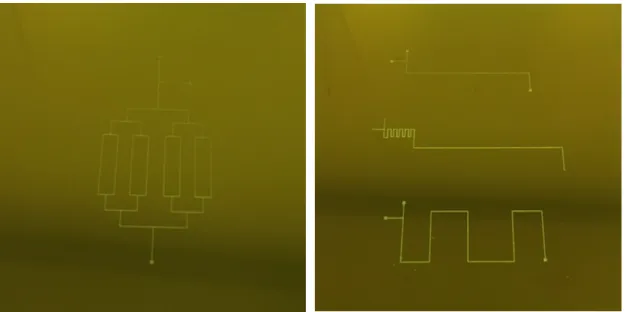
(a) Photomask for 8-branched microchan-nels.
(b) Photomask with single channels, differ-ent geometries.
Figure 3.1: Photomasks for microfluidic applications.
3.2.1
Mask Preparation
Photomasks, are usually made of transparent fused silica with a covered opaque chrome pattern, 5 by 5 inches, are used for obtaining desired shapes onto samples by using photolithography. Transparent sections allow UV light to pass through the sample. For this specific case, desired shapes are microchannels with different dimensions. They are prepared to obtain specific microfluidic applications, which are elucidated in the following sections, by using SOLIDWORKS and GDSII editor, namely K-layout, and taking into consideration the equipment limitations.
3.2.2
Preparation of the Master
Samples which are used as molds, usually referred as the Master, can be obtained by using negative photoresists, namely SU-8. Depending on the viscosity, there are different types of SU-8s that are commercially available. SU-8 used in the experiments is 2050, to obtain microchannels with different dimensions; 75µm
– 200µm in depth, 30µm – 200µm in width. First, a layer of HMDS, Hexam-ethyldisilazane, is spin coated with following parameters, Table 3.1, to form an adhesion layer between silicon wafer and the SU-8. SU-8 is spin coated in two steps, due to its viscous nature.
Table 3.1: Spin Coating Parameters for 200µm Resist HMDS 4000 rpm 40 seconds
SU-8 500 rpm 10 seconds SU-8 1000 rpm 30 seconds
For different devices, different thickness of SU-8 is also tried. Some of the devices are done with 75m thickness of SU-8, and spin coating parameters can be found at table3.4.
Table 3.2: Spin Coating Parameters for 75µm Resist HMDS 4000 rpm 40 seconds
SU-8 500 rpm 10 seconds SU-8 2000 rpm 30 seconds
After the spin coating process, there might be build up of the photoresist on the edges of the wafer. This excess photoresist should be removed by the help of acetone; to prevent the contamination of the hot plate during baking process. Additionally, this excess photoresist affects the homogeneity of the layer; which results with uneven exposure at the photolithography step. This process is also known as Edge Bead Removal.
In order to dry the coated resist and make it more resistant, soft bake step is needed. For viscous resists as SU-8, two step baking that is elevated is recom-mended. Baking time and temperature can be seen from Table 3.3.
3.2.2.1 Photolithography
After negative photoresist is spin coated onto the sample, in this case silicon wafer, photolithography is used to transfer desired patterns from photomask, with UV light. It has different pattern transferring techniques: First one is when the mask is in direct contact with the substrate. The second and preferred one for this fabrication is when there is a small proximity distance between the mask and the substrate, to avoid sticking between surfaces. Since the minumum feature size is in microns, it does not result in low resolution. The light changes photoresist’s chemical properties, and depending on the photoresist; negative or positive, the section of the photoresist that is exposed to light strengthens or loosens the bonds between their molecules.
In the case of SU-8, negative photoresist, exposure cross-links the bonds (Fig-ure 3.2). Some parameters that are used for photolithography application can be seen from Table 3.3.
Figure 3.2: Schematic of photolithography onto negative photoresist.
In addition to silicon, other materials as glass, pyrex, or silicon nitride can be used with different exposure doses.
For 75µm thickness of SU-8, photolithography parameters can be observed at Table 3.4.
Table 3.3: Photolithography Parameters
Soft Bake 65°C, 7 minutes 95°C, 33 min Exposure Type & Dose Proximity 275cmmJ2
Post Exposure Bake 65°C, 5 minutes 95°C, 13 min Table 3.4: Photolithography Parameters for 75µm thickness of SU-8
Soft Bake 65°C, 3 minutes 95°C, 9 min Exposure Type & Dose Proximity 200cmmJ2
Post Exposure Bake 65°C, 2 minutes 95°C, 7 min
After exposure, SU-8 layer must be heated again. This step is known as post exposure bake, and it is needed to accelerate the SU-8 polymerization. This step also reveals if the exposure is optimal or not, since visible latent image should be seen in the film after it is placed on the hotplate. Parameters can be seen from Table 3.3.
When the patterns are visible, SU-8 should be developed to form final struc-ture. This development can take place in commercially available SU-8 Developer, or diacetone alcohol; one of the solvent based developers. Depending on the thickness of the SU-8, development times may vary, and should be optimized. The time interval used for this work is approximately 16 minutes, and constant agitation is recommended. If the pattern has tight pitch or holes, ultrasonic bath may be used during development.
Final step in the cleanroom is curing the SU-8, also known as hard bake. This step is usually recommended for devices that will be subjected to thermal processing, since SU-8 is a thermal resin and its properties can change when exposed to high temperature levels. Baking for a couple of minutes at 150°C can strengthen the structures, hence it is useful for microfluidic applications.
In the cleanroom, not only 8-branched and single zigzag microchannels are fabricated. For different applications where small channel dimensions are needed, a single channel with a smaller width for particle experiments is also established.
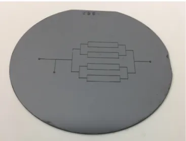
Figure 3.3: Si wafer with SU-8 structures; in this case a 8-branched microchannel. To use only 4-channels, a portion of SU-8 is removed from the mask.
Figure 3.4: Si wafer with SU-8 structure; namely a single microchannel geometry. Width of the channel is approximately 50µm.
As it is explained, in addition to silicon, other materials can be used with different exposure doses.
3.2.3
PDMS Preparation
After the SU-8 master is ready to use, sample is taken to laboratory to work with PDMS. This section can also be done in the cleanroom. PDMS is prepared by using Sylgard 184 Silicone Elastomer Kit, which also contains curing agent. By changing the ratio between the elastomer and the curing agent, desired Young’s Modulus, E, can be obtained. For this work, (10:1) is used. After the mixture is ready, it is put into vacuum desiccator to remove bubbles. These bubbles can solidify in the baked PDMS. Mixture is then poured onto the silicon wafer with SU-8 features,(where these features are the microchannels),and put in the oven
for 60 minutes, at 80°C, for cross-linking. Some of the PDMS that is prepared in this step is reserved to be used for the cooper sheets. The mixture can also be left at the room temperature for 24 hours.
When the PDMS is cooled down, it can be cut from the master wafer with a scalpel, and gently peeled off.(Figure 3.5) As it is explained above, this PDMS now has the microchannels that are needed to be bonded to form enclosed volumes. Since it is desired to add and remove fluids from the channels, inlet and outlet ports should be punched. The number of these ports can vary depending on the application. Due to the fact that PDMS is a soft material, ports can be gently punched out by using stainless steel punchers.
Figure 3.5: Silicon with SU-8 structures. A thin layer of PDMS is poured and baked.
3.2.4
Ground & Strip Layers
Ground and strip layers of the device is cut from a copper sheet, with a thickness of 500µm. Both layers are cut with guillotine shears, The ground plate has dimensions as 7cm x 10cm, and the strip is 0.1cm x 11cm. These parts are then polished, and ground layer is coated with the reserved PDMS, to form a thin layer, and baked.
(a) 8-branched device after the mi-crostrip line connection.
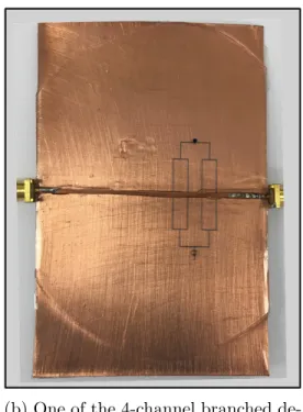
(b) One of the 4-channel branched de-vices.
Figure 3.6: Final products for different applications. Coloured DI water is filled in order to embellish the microchannels.
Device assembly is needed to form closed micro structures with specific vol-umes. In this work, plasma-activated bonding is used. It is a low temperature bonding technique and makes surfaces hydrophilic, namely the surfaces to be bonded will have similar characteristics, and removes contaminants.
After the ground layer is cooled down to room temperature, it is placed in air plasma chamber with the PDMS that has microchannel structures. Approxi-mately in 40 seconds, air plasma activates both surfaces. After activation process, both surfaces are carefully aligned and gently pressed together. Next, copper part that will serve as the microstrip line is aligned at the center of the device and attached to the device by using PDMS as adhesive layer. Finally the end product is baked in oven for 45 minutes. Fabrication steps can be also seen from Figure 3.7.
To have electronic connection; actuation and read-out, microstrip line is bent down from both sides, touched to the ground layer. The device is grounded to
Figure 3.7: Fabrication schematic of the device.
obtain a specific boundary condition hence to have a specific mode shape, which is explained at the previous chapter. SMA ports are soldered from both sides of the device.
Figure 3.8: Final product for a device with a zigzag microchannel.
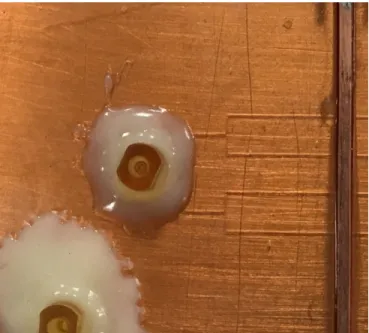
To deliver and collect fluids, inlet and outlet ports are used. There are two main approaches that are used for these applications. The first one is using capillary tubing (OD: 360µm, ID : 160µm). As it can be seen from Figure 3.9, some of the devices have inlet and outlet ports for capillary tubing connections. These ports are placed with Epoxy, and the device is left at the room temperature for 24 hours.
Other method is using PTFE tubing, (OD:1.2mm). For PTFE tubing, there is no need to have other parts as connectors, it can directly be used with PDMS based devices. In general, for droplet experiments, capillary tubing is used; and
for cell experiments, PTFE tubing is used.
Figure 3.9: Port connector with epoxy. 4 branch of microchannels and microstrip are also visible.
Chapter 4
Droplet Detection with
Microstrip line Resonator
As it is introduced at previous chapters, Lab-on-a-Chip applications gain impor-tance due to their capability of performing chemical, biological and nanotech-nological applications within small volumes. This chapter introduces droplet microfluidics, and how it is used with microstrip line resonators integrated with microfluidics.
In this work, microdroplets are formed and used in the experiments with mi-crostrip line resonators, for size and position determination. To do the experi-ments, two microchannel models are used: The first channel design is based on a zigzag channel; where channel crosses signal line at 6 different locations. The second channel design is branched channels into 4, in order to sort droplets; in other words, send the droplets from different channels that are at different loca-tions, by using hydraulic resistance. This part of the work will be investigated in the following sections.
4.1
Droplet Microfluidics
Droplet microfluidics is one of the main approaches that manipulates fluids at miniaturized platforms to perform mainly biological and chemical applications. Droplets are formed by two immiscible fluids, in laminar flow regime[37]. These manipulations take place in microdroplets, where their dynamical properties as the temperature, position and concentration must be maintained. For chemical experiments, it is favorable due to the fact that droplets can be manipulated independently and thus serve as individual reaction units[38]. It has also usage in cell and synthetic biology, due to high throughput. Cells can be loaded into droplets, and applications as cell counting or cell manipulation can be achiev-able. Other techniques as using microwells with a picoliter volume can also be adapted. However, these approaches can be difficult due to capillary effects at small dimensions[39]. Integration with other fields, especially cell biology makes droplet microfluidics more favourable. In this study, T-junction method is used to produce water droplets in oil. Here, oil is used for the continuous flow, and water is used for the disperse flow. For microfluidics applications, flow rate of the continuous flow is at most upto 50 µL
min. There are some parameters that are involved with droplet generation, and they are introduced briefly at upcoming sections.
To prevent droplets to merge into one, a chemical called surfactant can be added to the continuous phase, to minimize the surface tension. For this work, surfactant is not used.
Since the continuous fluid is chosen to be oil, and water droplets should not wet the channel walls, hydrophobic walls are needed.
4.1.1
Capillary Number
During droplet formation, most important forces are viscous force, and interfacial tension. Capillary Number, Ca, is a quantity that compares strength of viscous
force to interfacial force, surface tension. It should be monitored to gain a sight about the droplet dimensions, and formation rates [38].
Ca = µv
γ (4.1)
Where µ is the viscosity and v is the velocity of the continuous fluid, γ is the surface tension between two phases.
There are three flow regimes, based on Capillary number. First regime is known as squeezing, where Ca is low. The second one is dripping regime, where viscous shear force dominates tension, and droplets are formed before disperse phase moves to the junction area. The final regime is the jetting, where Ca is high, and it seems as the disperse phase elongates along the channel for a portion. In this work, flow rates are determined in order to obtain single, rather slow droplet to track the frequency shift that is caused by this droplet, while it is passing under the signal line.
4.1.2
Flow Rate Ratio
In order to obtain homogeneous droplets with same sizes, the ratio between the flow rate of the continuous phase to disperse phase is important. To cite an example, for a large flow rate ratio and large flow rate of the disperse phase, the droplet can be in the jetting regime, which results in a large droplet, and many small droplets. In order to decide the ratio, firstly, a set of simulations are done. At the end of the simulations, flow rate of the oil (continuous phase) is decided to be greater than the water (disperse phase). A more delicate adjustment is done by experimental trials hence, flow rate ratio is determined by the end of these trials (Table 4.1). Since single droplet is needed to travel the microchannel before disturbance of other droplets, flow rates are rather slow.
Table 4.1: Flow Rates of the Continuous and Dispersed Flows Continuous Flow( µL
min) Dispersed Flow ( µL min) 0.5 0.05 0.6 0.03 0.5 0.1 0.9 0.2
4.1.3
Geometry
Geometry of the channels is important, since it will directly affect the size of the droplets. For example, with the same flow rates and ratio, with smaller widths, smaller droplets will be formed, compared to wider channels. Another thing is that, with smaller channel dimensions, hydraulic resistance will be higher, which causes droplets to flow through other inlet; rather than the channel that will lead to outlet port.
4.1.4
T-Junction for Droplet Formation
Another geometric concern is the droplet formation junction. Droplet formation can be classified into coflow, cross-flow, and flow-focusing categories[40]. One of the methods to form droplets is using so called T-junctions, one of the cross-flow junctions. In this work, it is preffered, and schematic can be seen at Figure 4.1. This junction produces droplets hydrodynamically. To deliver oil and water and form droplets, two syringe pumps are used. Two different flows meet at an angle[41], usually this angle is orthogonal. Droplets are formed as described: Disperse phase, blokes the continuous phase, forms shear gradient, and it is broken into droplets.
Although T-Junction is one of the most used geometry to form droplets, there are other geometries for different applications as K-Junction[42], V-Junction[43].
(a) Schematic. (b) Microscope image.
Figure 4.1: T-Junction for droplet formation. Water droplets are formed with carrier fluid, oil.
In this study, it is chosen since it is easy to fabricate, and it can produce mono-disperse droplets.
There are also active methods to form droplets, where external forces are applied. There are electromechanical, magnetic and thermal methods. One of the methods is called as EWOD, Electrowetting-on-Dielectric, where electrical field is applied to reduce the contact angle between the flow and the channel[44].
4.2
Droplet Detection with a Zigzag
Microchan-nel
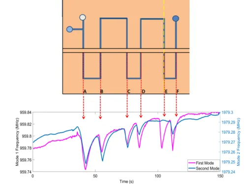
To send microdroplets which are formed in a T-Junction, a Zigzag channel geome-try is used. The reason to use such a geomegeome-try is due to the fact that microchannel crosses signal line at 6 different positions. At each position, frequency shifts on
considered modes, first and the second modes for this case, will differ, and they can be seen at Figure 4.2. One of the reasons that causes frequency shifts is the difference between the relative permittivity of the water(approximately 78.3 [45]), and the olive oil(approximately 2.5 [46]) at microwave frequency band, room tem-perature. Each crossing point is labelled from A to F, and the total length of the device is 99.79mm. Point E is approximately at the center of the device. The positions of the crossings are given at Table 4.2.
Figure 4.2: Frequency shifts on first and second modes due to droplet passage. Point E is approximately at the center of the device.
A single water microdroplet in olive oil is formed and send to the microchannel by syringe pumps. The flow rates for disperse and continuous flows are Qwater =
0.03 µL
min and Qoil = 0.6 µL
min. These rates are set after the channel is filled with water, manually, so that a slow single droplet can be formed.
Table 4.2: Normalized Positions of the Microchannel Sections Where They Cross the Signal Line.
Point A Point B Point C Point D Point E Point F 0.192mm 0.277mm 0.36mm 0.438mm 0.518mm 0.599mm
4.3
4-Branched Microchannels for Droplet
Dis-tribution, Location and Electric Volume
Calculations
The reason to use 4-branched microchannel is to sort droplets; namely distribute them into different channels. It is necessary for selection and segregation of droplets; and this system can be used for further analysis[47]. For the mentioned work, since each channel crosses the signal line at different positions, this concept is needed to test the multimode sensing for position characterization[30], (Figure 4.3). There are mainly two sorting mechanisms: Active and passive. One of the main active methods is using electrophoresis[48]. In this work, passive sorting due to hydraulic resistance is investigated.
As is stated above, due to hydrodynamic resistance that is caused by the chan-nel geometry and passage of the earlier droplets, 4-branched chanchan-nel structure is used. Resistance analogy is similar with electrical circuits, whereas the flow rate is similar to current, pressure difference replaces voltage difference, and hydraulic resistance is similar to the resistance of an electrical circuit.
4P = QRhydraulic (4.2)
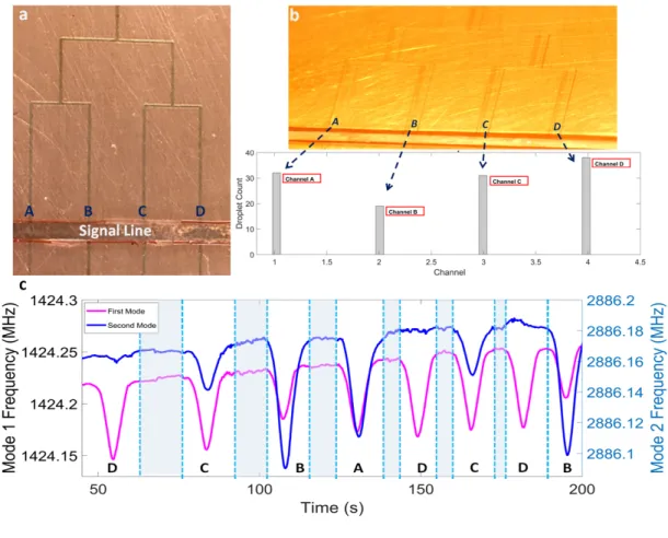
After a set of experiments, it is seen that droplets are dispersed almost randomly through the channels[30], Figure 4.3. Channels are labelled from A to D, where channel D is at the center of the microwave resonator. Histogram of the droplets can also be seen at Figure 4.3. The histogram is plotted by using 121 droplet passages, and it can be seen that channel B is less favourable than other chan-nels. The reason for that is the fabrication defect: Channel B already has more resistance than the other channels, due to excess SU-8.
Frequency shifts that are originated from droplet passages are visible in Figure 4.3. Due to their location, each droplet creates different frequency shifts. For example, a droplet that passes through channel D, the channel which is located at the near-center of the device, induces different frequency shifts on both modes.
Figure 4.3: (a)4 microchannels that are used for droplet distribution. (b)Histogram of 121 droplets and their choice of microchannels. (c)Frequency shifts on both modes, due to droplet passage from one of the channels, A to D.
The reason for this is due to the fact that the amplitude of the electric field for the first mode is high at the center and second mode has antinode at the same location (due to their mode shapes and boundary conditions).
The path that the droplets follow can be examined from Figure 4.4. In this figure, a junction that is divided into two channels and 2 droplets that are con-secutive can be seen. The first droplet, indicated with black circle, favours the least resistive path. Since the first droplet increases the hydraulic resistance, the second droplet, indicated with red circle, goes towards the other channel; which has lower hydraulic resistance. Therefore, only one microdroplet passes through the sensing region of the sensor, at any given time [30].
Figure 4.4: Droplet sorting by branching the microchannels. Two droplets are visible. Second droplet favours channel with lower hydraulic resistance.
The normalized locations of the channels with respect to the length of the resonator are 0.297cm, 0.365cm, 0.426cm and 0.493cm. These locations can be calculated from frequency shifts, as can be seen at Figure 4.5. For the study, they are measured beforehand the experimental trials, and compared with the results. When the frequency shifts on both modes are plotted, position values can be found as straight lines that pass through origin. Each position has different lines with different slopes [30],[20]. Additionally, position histogram can be examined for the comparison between actual and experimental data, at Figure 4.6. After location data is obtained, electrical volume of the droplet can also be calculated.
Figure 4.5: Position data of the droplets in frequency shift domain. Inset also shows how position and electrical volume contours are calculated. Reprinted with permission of Royal Society of Chemistry, Lab on a Chip Journal, Issue 3, 2018.[30]
(a) Position histogram. (b) Electrical volume histogram.
Figure 4.6: Droplet information. Reprinted with permission of Royal Society of Chemistry, Lab on a Chip Journal, Issue 3, 2018.[30]
As evident from Figure 4.6, even though droplets pass from different mi-crochannels, electrical volume histogram has a sharp peak. The reason for this is the fact that the produced droplets have similar sizes. Size can be calculated from the electrical volume; it is the volume of the droplet times the dielectric constant difference between the continuous flow and the droplet[30]. Hence, droplets which pass through different channels indeed have the same electrical volume properties.