Reduced facet temperature in semiconductor lasers using electrically
pumped windows
Abdullah Demir
1*, Seval Arslan
2, Sinan Gündoğdu
2, Atilla Aydınlı
31
Bilkent University, UNAM - Institute of Materials Science and Nanotechnology, Ankara 06800,
Turkey
2
Bilkent University, Department of Physics, Ankara 06800, Turkey
3
Uludağ University, Department of Electrical and Electronics Engineering, Bursa 16059, Turkey
ABSTRACT
The self-heating of semiconductor lasers contributes directly to facet heating and consequently to the critical temperature for catastrophic optical mirror damage (COMD) but the existing facet engineering methods do not address this issue. Targeting this problem, we report experimental and modeling results that demonstrate a new method achieving facet temperatures significantly lower than the laser cavity temperature in GaAs-based high-power semiconductor lasers by using electrically isolated and pumped windows. Owing to monolithic integration, the method does not introduce any penalty on the efficiency and output power of the laser. Thermal modeling results show that the laser output facet can be almost totally isolated from heat generated in the laser cavity and near cold-cavity facet temperatures are possible. The method can be applied to single emitters, laser bars, and monolithically integrated lasers in photonic integrated circuits to improve their reliability and operating performance.
Keywords: semiconductor laser, high power laser diode, catastrophic optical mirror damage (COMD), facet temperature,
facet cooling
1. INTRODUCTION
Semiconductor lasers with reliable high output power are of great interest to many applications, especially recently for direct-diode and fiber lasers with kW-level output used in material processing [1]. The reliability and performance of these high-power systems are backed up by the reliability of the single emitters. Although laser powers exceeding 30 W from a 100 µm wide broad area laser have been demonstrated [2, 3], the operating output power of these devices are much lower (i.e. below 20 W) due to reliability limitation. Catastrophic optical mirror damage (COMD) of the output facet is a key failure mode that constrains the device reliability and scaling of the operating laser power [4]. COMD is a heating induced device failure mechanism and even higher operating laser powers may be possible if it can be avoided.
Despite a variety of methods used for facet passivation and engineering [5], and high electro-optical power conversion efficiencies of these devices, the temperature rise at the facets limits the reliability and operating power of high power edge emitting semiconductor lasers. Facet heating leads to the bandgap shrinkage and further facet absorption resulting in COMD. Many successful methods were reported in the literature to prevent facet mirror reaching the critical temperature of Tc=120-160 oC that triggers COMD on the output facet [4]. These methods limit the temperature increase of the output
facet and, consequently, its optical strength against COMD is improved. Non-absorbing mirrors (NAMs) and unpumped windows near output facets have been employed to reduce optical absorption and facet heating [6, 7]. NAMs produced by quantum well-intermixing is a complex process with tight fabrication tolerances. In the unpumped window method, facet temperature was shown to be lower using ~30 µm long current blocking region due to reduced current density near facet [8]. Alternatively, ultra-high vacuum cleaving and passivation of the facets eliminates the surface states for higher COMD thresholds at the cost of higher complexity and expense of fabrication [9]. These approaches have accomplished effective results increasing Tc. Although eliminating the surface recombination and optical absorption are important to limit the
facet heating as targeted in the previous studies, the self-heating of the laser cavity contributes directly to facet heating and Tc, and it is probably the dominant source of facet heating. However, the existing methods have not addressed this issue
before. Targeting this problem, we report experimental and modeling results that demonstrate a new method [10, 11] achieving facet temperatures significantly lower than the laser cavity temperature in 9xx-nm high power semiconductor
lasers by using electrically isolated and biased transparent windows. Integrating long transparent window regions, where the transparency is controlled by applied bias with very low injection current, the self-heat load of the laser cavity can be thermally isolated from the output facet. Facet temperature was reduced by 40% compared to that of the control sample. Reduced facet temperatures are even below the laser cavity temperature demonstrating facet cooling. The thermal modeling of the devices shows that the facet temperature of a semiconductor laser can be reduced significantly and near cold-cavity facet temperatures are possible. Owing to monolithic integration, the method does not introduce any penalty on the power conversion efficiency and output power of the lasers.
2. EXPERIMENTAL DETAILS
The standard and new two-section laser approach are schematically compared in Fig. 1. A two-section chip is divided into two regions by separating the top electrode into laser and window sections. The laser cavity can operate at high current levels and therefore generates very high heat. The bulk temperature of the high-power laser diodes increases due to the dissipated power, and hence, for a standard laser, the facet temperature can be even higher than the laser cavity. In contrast, in a two-section laser, the window section next to the facet, is biased to transparency and, so, operates at very low current levels with negligible heat generation. Such a device configuration allows keeping the high heat load of the laser cavity away from the heat sensitive output facet. By extending the cold laser output window, the heat generated in the laser section can be separated from the output facet.
Figure 1. The schematic illustration of the side view of (a) standard single section laser, (b) developed two-section laser.
The epitaxial structure of our GaAs-based laser emitting at 915 nm is composed of 3000 nm n-AlGaAs cladding, 500 nm n-AlGaAs waveguide, single InGaAs quantum well layer, 500 nm p-AlGaAs waveguide, 1000 nm p-AlGaAs cladding and 100 nm GaAs contact layer [12]. In this work, 5 mm long and 100 μm wide broad area high power laser diodes with standard single-section and proposed two-section lasers were used to compare their performance and facet temperatures. Both lasers have 50 µm unpumped current blocking windows near facets to prevent facet absorption due to excess carriers. No facet passivation and mirror coatings were applied. 200 nm thick Si3N4 layer was deposited for passivation and
unpumped windows. The two-section laser have trenches for electrical isolation between the laser and window sections so that they can be biased independently. We limited the depth of the isolation trench to 300 nm to preserve the mode profile and not to introduce optical losses. The electrical resistance between the lasing and window sections of two-section laser was measured as 69 Ω, which is >1000 higher than the series resistance of the laser. Hence, the carrier leakage between the laser and window sections is negligible. The lasers were cleaved and mounted epi-up on Cu-blocks.
Laser performance was evaluated under CW operation at room temperature for uncoated and epi-up lasers to simplify the
observation of the facet cooling. The electro-optical power conversion efficiency of the lasers is around 52% that is limited
by uncoated facets and epi-up operation. As shown in Fig. 2, The dependence of the single-facet output power on the laser current is compared for the standard (5 mm)x(100 μm) and (4 mm + 1 mm)x(100 μm) two-section lasers, where 1 mm is the length of the window section, at various window bias current levels. The power loss is around 15% when no bias is applied to the window section. The transparency and threshold current (Ith) of 1 mm long cavity of our laser structure is
estimated to be 76±7 mA and 257±28 mA, respectively, using basic laser rate equations [13]. By applying an above-transparency injection current of 100 mA, the output power is recovered confirming that the absorption loss of the window section is eliminated, and transparency is established. The threshold current of the 5 mm long laser is 568 mA whereas the
threshold current of 4+1 mm two-section laser with Iwin=100 mA is 463 mA. This shows that the sum of the Ith and Iwin of
the two-section laser is approximately equivalent to the Ith of the standard laser for the same total device length. The
threshold current of the two-section laser decreases with an increase of the window section bias current since the spontaneous emission in the window section contributes to the gain in the laser section. Hence, the sum of Ith and Iwin gives
the actual threshold current of the two-section lasers.
Figure 2. The front facet laser output power vs. laser current for the standard and two-section laser (Iwin=0 and 100 mA).
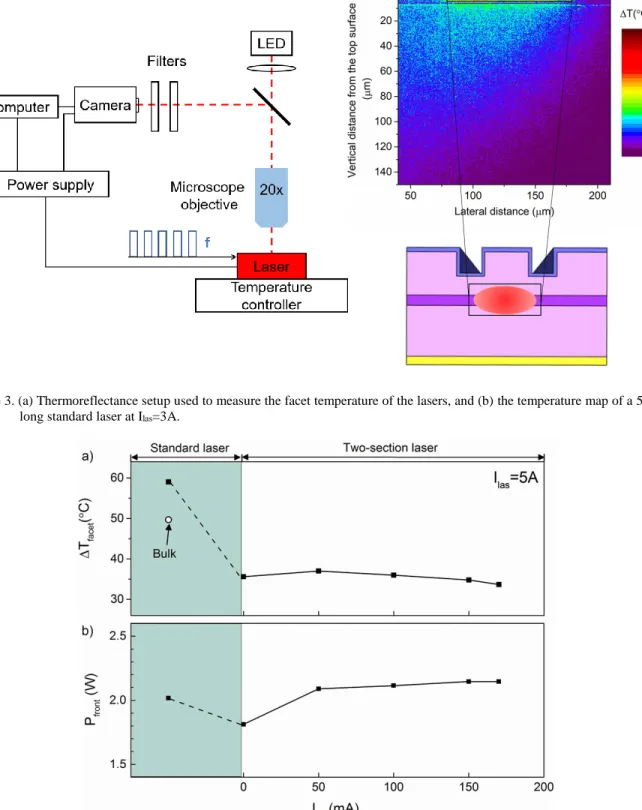
Facet temperatures of the standard and two-section laser diodes were compared for emitters on the same bar. CMOS-based
thermoreflectance method [14, 15] shown in Fig. 3(a) was used to obtain the temperature map of the facets. An LED at 450 nm was used as a probe light and directed onto the laser facet through a microscope objective (20x, 0.40 NA). Lasers
were tested at room temperature up to 5 A laser injection current (Ilas). A current source diode driver (LDX-3600) was used
under QCW current injection with 20 ms pulse duration and 20% duty cycle. Two-section lasers were tested under various
Iwin of 0, 50, 100, 150, 170 mA and lasing current of Ilas. The temperature modulated back-reflected light was collected
with a CMOS camera triggered by a diode driver and analyzed by a computer. The relative change in reflectivity was correlated with the temperature change given as
∆𝑅 𝑅 = ( 1 𝑅 𝜕𝑅 𝜕𝑅) ∆𝑇 = 𝜅∆𝑇
where 𝜅 is the thermoreflectance coefficient and it depends on the laser material and probe light wavelength [14], R is the reflectivity of the sample material and T is the temperature. For the GaAs substrate of our laser structure, 𝜅 was measured
as (3.2±0.6)×10−4 at 450 nm by modulating the laser temperature using a temperature controller. For our purpose of
comparing the facet temperatures of standard and two-section lasers, possible differences between 𝜅 of GaAs and epitaxial
layers of the laser structure are not critical. Our measurements had 0.1oC temperature and 0.7 μm spatial resolution. The
spatial resolution allows us the characterize the temperature increase around the active region of the waveguide. Fig. 3(b)
shows the facet temperature measurement result as a map for a 5 mm long standard laser at Ilas=3A. The active region has
the highest temperature and heat spreads out both vertically and laterally. It is also clear that the right-hand side of the structure is cooler than that of the left due to its larger spacing from the edge of the chip compared to that of the left.
Figure 4(a) shows the temperature rise of the facet in the active region for the standard and two-sections lasers and compares them to the bulk of the laser cavity at 5A. Facet temperature for the standard laser increases by 59oC, which is
higher than its bulk temperature increase of 50oC, as expected due to other contributions to the facet temperature such as
non-radiative surface recombination and edge effects. For the two-section laser, the facet temperature increase stays below 37oC and reaches as low as 34.7oC at 170 mA of window current. Starting at I
win=100 mA, which is above the estimated
transparency current of 79 mA, the facet temperature decreases slightly since optical absorption loss induced heating in the window is expected to be eliminated. Even though integrating a cold region between the laser and facet provides
significant temperature reduction for the facet, it introduces an output power penalty if not biased above its transparency as shown in Fig. 4(b). The temperature is reduced by 40% at the facet and 30% compared to the bulk using the 1 mm long transparent window at 5A laser injection current with Iwin=170 mA.
Figure 3. (a) Thermoreflectance setup used to measure the facet temperature of the lasers, and (b) the temperature map of a 5 mm long standard laser at Ilas=3A.
Figure 4. Comparing the active region facet temperature increase and front facet output power of standard, (5 mm)x(100µm), and two-section, (4 mm + 1 mm)x(100 µm), laser devices.
Fig. 5 presents the magnified facet temperature map of the active region for both standard and two-section lasers. It shows that the standard laser has large temperature fluctuations (ΔTav=59±3.0 oC) and two-section laser has more homogenous
temperature fluctuations (ΔTav=34±0.4 oC). Note that the temperature fluctuations in the standard laser reaches ΔTpeak=130 oC whereas the it is much lower, ΔT
peak=45 oC, in the two-section laser facet. Both the magnitude of the temperature and
its fluctuations show that the two-section laser has much cooler and stable facet temperatures than the standard laser.
3. THERMAL MODELING
We simulated the temperature distribution of two-section lasers using the heat transfer module of COMSOL. A heat source representing the dissipated power is placed in the active region of (4 mm + Lwin) long laser. The facet absorption is not
considered in the simulations as it is difficult to quantify. The thermal resistance of the laser is assumed to be 2.5 K/W and 5 K/W, which represents typical values for broad-area high power laser diodes [2]. Fig. 6(a) shows COMSOL thermal modeling results of the two-section laser with a high heat load of 20 W that corresponds to a high current operation for such a laser [2, 16]. For thermal resistance value of 2.5 K/W, which can be achieved by epi-down soldering, laser section
(a) (b)
Figure 5. Magnified facet temperature map around the active region for (a) standard laser shows ΔTav=59±3.0 oC with ΔTpeak=130 oC and (b) two-section laser shows ΔTav=34±0.4 oC with ΔTpeak=45 oC.
Figure 6. Using a heat load of 20 W, thermal modeling results for (a) facet temperature increase vs. pumped window length for two different thermal resistance values, (b) temperature map for low thermal resistance device with 1 mm long window.
contributes less than 1oC to the facet temperature using a 1 mm long transparent window. This is a substantial reduction
of the facet temperature compared to 50oC for the standard laser diode configuration. It shows that the facet temperature
can be reduced by 93-99% (i.e. up to ~100x) by using 1-2 mm long windows. The top view for the temperature map of this laser is given in Fig. 6(b). As seen from the map, the heat generated by the laser region diffuses longitudinally towards the facet through the cold window. The simulated design is similar to our fabricated lasers and it shows an asymmetric temperature distribution as obtained in the thermoreflectance measurement results presented in Fig. 3(b). As the length of the window section increases, the facet temperature decreases. The data suggest that longer windows are required for higher thermal resistance devices to keep the laser heat contribution to the facet low.
4. CONCLUSION AND OUTLOOK
We have demonstrated a promising method for facet temperature reduction for semiconductor lasers using electrically injected transparent windows without compromising the laser performance. The method is based on a monolithic cavity with laser and window sections, where the window is biased to transparency to eliminate its absorption losses. The facet temperature of a two-section laser is reduced even below its laser cavity temperature using a 1 mm long transparent window. The COMSOL modeling shows that the facet heating due to dissipated power of the lasing region can be almost totally eliminated. The method is general enough to be implemented in a variety of semiconductor lasers and we anticipate that the presented approach could lead to stronger laser facets against COMD and improved device operating lifetime.
5. REFERENCES
[1] E. Zucker, D. Zou, L. Zavala, H. Yu, P. Yalamanchili, et al., “Advancements in laser diode chip and packaging technologies for application in kW-class fiber laser pumping,” Proc. SPIE 8965, 896507 (2014).
[2] A. Demir, M. Peters, R. Duesterberg, V. Rossin, and E. Zucker, “Semiconductor laser power enhancement by control of gain and power profiles,” IEEE Photon. Technol. Lett. 27, 2178 (2015).
[3] V. Gapontsev, et.al, “Highly-Efficient High-Power Pumps for Fiber Lasers,” Proc. SPIE 10086, 108604-1 (2017). [4] J. W. Tomm, M. Ziegler, M. Hempel, and T. Elsaesser, “Mechanisms and fast kinetics of the catastrophic optical
damage,” Laser Photonics Rev., vol. 5, no. 3, pp. 422-441, 2011.
[5] P. W. Epperlein, “Semiconductor laser engineering, reliability and diagnostics: a practical approach to high power and single mode devices,” Wiley, 2013.
[6] P. G. Piva, S. Fafard, M. Dion, M. Buchanan, S. Charbonneau, R. D. Goldberg and I. V. Mitchell, “Reduction of InGaAs/GaAs laser facet temperatures by band gap shifted extended cavities,” Appl. Phys. Lett., vol. 70, no. 13, pp. 1662-1664, 1997.
[7] J. Michaud, P. D. Vecchio, L. Béchou, D. Veyrié, M. A. Bettiati, F. Laruelle and S. Grauby, “Precise facet temperature distribution of high-power laser diodes: Unpumped window effect,” IEEE Photon. Technol. Lett. 27, 1002 (2015). [8] F. Rinner, J. Rogg, M. T. Kelemen, M. Mikulla, G. Weimann, J. W. Tomm, E. Thamm and R. Poprawe, “Facet
temperature reduction by a current blocking layer at the front facets of high-power InGaAs/AlGaAs lasers,” J. Appl. Phys. 93, 1848 (2003).
[9] L. W. Tu, E. F. Schubert, M. Hong and G. J. Zydzik, “In-vacuum cleavingand coating of semiconductor laser facets using thin silicon and a dielectric,” J. Appl. Phys. 80, 6448 (1996).
[10] Patent pending.
[11] S. Arslan, S. Gundogdu, A. Demir, and A. Aydınlı, “Facet cooling in high power InGaAs/AlGaAs lasers,” IEEE Photon. Tech. Lett. 31, 94 (2019).
[12] S. Arslan, A. Demir, S. Şahin and A. Aydınlı, “Conservation of quantum efficiency in quantum well intermixing by stress engineering with dielectric bilayers,” Semicond. Sci. Technol. 33, 025001 (2018).
[13] T. R. Chen, L. E. Eng, Y. H. Zhuang, and A. Yariv, “Experimental determination of transparency current density and estimation of the threshold current of semiconductor quantum well lasers,” Appl. Phys. Lett. 56, 1002 (1990). [14] M. Farzaneh et al., “CCD-based thermoreflectance microscopy: Principles and applications,” J. Phys. D: Appl. Phys.
42, 143001 (2009).
[15] D. Pierścińska, “Thermoreflectance spectroscopy—Analysis of thermal processes in semiconductor lasers,” J. Phys. D: Appl. Phys. 51, 013001 (2018).
[16] A. Demir, M. Peters, R. Duesterberg, V. Rossin, and E. Zucker, “29.5W continuous wave output from 100 μm wide laser diode,” Proc. SPIE 9348, 93480G (2015).