High-refractive-index measurement with an
elastomeric grating coupler
Askin Kocabas, Feridun Ay, Aykutlu Dâna, Isa Kiyat, and Atilla Aydinli Türk Telekom Bilkent Laboratory, Department of Physics, Bilkent University, 06800 Ankara, Turkey
Received May 26, 2005; revised manuscript received August 2, 2005; accepted August 8, 2005 An elastomeric grating coupler fabricated by the replica molding technique is used to measure the modal indices of a silicon-on-insulator (SOI) planar waveguide structure. Because of the van der Waals interaction between the grating mold and the waveguide, the elastomeric stamp makes conformal contact with the waveguide surface, inducing a periodic index perturbation at the contact region. The phase of the incident light is changed to match the guided modes of the waveguide. The modal and bulk indices are obtained by measuring the coupling angles. This technique serves to measure the high refractive index with a precision better than 10−3and allows the elastomeric stamp to be removed without damaging the surface of the waveguide. © 2005 Optical Society of America
OCIS codes: 050.2770, 130.2790.
Many multilayered material systems are being used for the realization of optical devices in which accu-rate knowledge of the refractive index at the operat-ing wavelength is crucial for proper design. Further-more, compact integrated optical components make use of high-index-contrast materials, which allow for smaller devices with lower radiation losses.1,2 Typi-cally, type III–V compound semiconductors grown by molecular beam epitaxy or metal-organic chemical-vapor deposition, silicon nitride and oxynitride mul-tilayers, as well as amorphous and crystalline silicon are used for such devices. A particular example is the silicon-on-insulator (SOI) waveguide structure with an index difference of ⬃2. Because of its high index contrast and compatibility with CMOS technology, an SOI structure provides an excellent platform for fab-rication of a variety of integrated optical devices on a single chip. It is commonly used in the fabrication of SOI-based polarization splitters, modulators, and ring resonators.3 Realization of all these devices re-quires an accurate knowledge of the refractive index with a precision better than 10−3.
Prism and grating couplers are used in the most common techniques for the measurement of the re-fractive indices of slab waveguides. Prism coupling of light into the planar waveguide requires a precisely calibrated prism with a refractive index larger than that of the material to be measured, as well as pres-sure applied to bring the prism into close proximity of the surface to be measured.4 High-index prisms are hard to fabricate, are expensive, and break easily un-der pressure. Grating couplers fabricated on the sur-face of the planar waveguide have also been used for the measurement of refractive indices in waveguide structures.5,6 Fabrication of a grating on the wave-guide structures with submicrometer periodicity re-quires the use of interference lithography techniques or sophisticated electron beam technology. Once fab-ricated, it is impossible to remove the grating with-out damaging the waveguide structure. A prism– grating combination has also been employed.7
Here, we report a new nondestructive and revers-ible technique for the accurate measurement of high refractive indices. This technique is based on the
cou-pling of free-space light to the guiding modes of a pla-nar optical waveguide by using an elastomeric stamp having a grating structure on its surface. The mea-surement of the coupling angles allows the determi-nation of the modal refractive indices. The SOI wave-guide structure was chosen to demonstrate the feasibility of the method.
The grating structure is one of the most fundamen-tal devices in integrated optics, based on periodic modulation of the refractive index on the surface of the waveguide.8When used to couple free-space light, the wavenumber of the incoming light can be changed during the coupling process. This coupling phenomena is governed by the Bragg equation,
kf,i= k0sin共i兲 + m2
⌳ , 共1兲 where k0, ,⌳, and kf,i are the wavenumber and the
angle of incidence of the propagating light, the peri-odicity of the grating, and the wavenumber of the guided modes, respectively. With the proper choice of the grating period,⌳, Eq. (1) is satisfied at particular coupling angles appropriate for different guided modes of the waveguide, from which one can calcu-late the modal indices.
In this technique, the periodic perturbation is cre-ated by making use of an elastomeric grating. A grat-ing stamp is fabricated by a micromoldgrat-ing technique. The micromolding technique has been extensively used for various optical applications.9–12The fabrica-tion procedure is shown in Fig. 1. A master grating prepared by interference lithography on a silicon wa-fer was used as a template. The periodicity of the grating was chosen to be 600 nm. Polydimethylsilox-ane (PDMS) in liquid form was poured onto the tem-plate, and a polished wafer was placed on the top sur-face with rigid separators in order to fabricate planar, smooth surfaces. Then the liquid PDMS was cured at 70°C for 3 h. In order to prevent the collapse of the depressions during contact, we chose a square wave profile for the grating shape with an etch depth of 200 nm. After the elastomeric grating stamp is peeled from the silicon surface, it is placed on the SOI
3150 OPTICS LETTERS / Vol. 30, No. 23 / December 1, 2005
waveguide structure. Because of the van der Waals interaction13between the PDMS and the Si surface, the grating stamp makes conformal contact with the SOI waveguide surface and induces a periodic change in the effective index of the waveguide. Due to ther-mal contraction, there is a 1% decrement in the peri-odicity of the PDMS grating. A possible partial lat-eral collapse of the PDMS during contact may cause a small variation in the periodicity also.14The peri-odicity of the grating stamp was measured by placing the grating surface on a glass wafer and measuring the deflection of the diffracted laser beams. Sinusoidal- and triangular-shaped grating stamps were also tried. However, owing to the low Young’s modulus, these submicrometer features collapsed during contact.15It has been shown that the collapse and distortion of stamps can be reduced by using a composite stamp of hard PDMS (h-PDMS).16
We applied the measurement technique to a Uni-bond SOI (SOITEC, France) wafer with a top Si thickness of 1.500± 0.020m and a 1m oxide buffer layer. A schematic of the experimental setup is shown in Fig. 2. The PDMS grating, placed on a SOI wafer, was mounted on a computer-controlled, motor-ized rotational stage with a step size of 0.005°. A la-ser beam from a 20 mW single-mode distributed-feedback laser operating at 1.568m was used to illuminate the sample. Zero-angle adjustment was done by aligning the backreflected beam with the in-cident one. The angular orientation of the grating was also tuned by aligning the zeroth- and first-order diffracted beams by using an infrared viewer. By sweeping the angle of incidence, all the guiding modes in the Si waveguide can be excited. The light
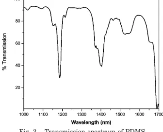
transmitted by the waveguide is monitored at the output of the waveguide by a large-area Ge detector. In order to assess the effects of material absorption of PDMS on the measurement, we measured the trans-mittance of a 1 cm thick PDMS layer using a Cary5 UV–VIS spectrophotometer. The measured transmis-sion spectra is shown in Fig. 3. Despite several strong CuH bands in the spectra, we find that the trans-mission in the vicinity of 1.568m is approximately 75%. This gives a tolerable intrinsic material loss of PDMS, ⬃1.5 dB/cm at the wavelength of 1.568m. The size of the PDMS grating stamp is 1 cm⫻1 cm. Coupling is achieved close to the edge of the stamp to prevent outcoupling. The guided mode propagates through only 2–3 mm in the PDMS region and about 3 cm in the SOI waveguide with air cladding. The re-sistivity of the Si top layer is 14–22⍀ cm, so the in-trinsic absorption loss is negligible at=1.568m.
Experiments were performed for both TE and TM polarizations. As a typical example, the experimental data for TM polarization are shown in Fig. 4. The TE spectrum is similar. Each peak corresponds to the ex-citation of a guided TM mode. The modal indices can be calculated from the Bragg equation. Index pertur-bation due to PDMS stamp is ⌬n=3⫻10−4 for the Fig. 1. (Color online) Schematic diagram of the
elasto-meric grating fabrication. (a) Silicon master grating, (b) casting and curing of liquid PDMS, (c) peeling of the cured elastomeric grating, (d) AFM image of the elastomeric grat-ing stamp.
Fig. 2. Schematics of the experimental arrangement for refractive index measurement using elastomeric grating coupler.
Fig. 3. Transmission spectrum of PDMS.
Fig. 4. Relative output power of the guided modes for TM polarization as a function of incident angle.
zeroth mode and increases with the mode number. The modal indices have been deduced from the mea-sured effective indices by using the approach de-scribed in Ref. 5, and the results are listed in Table 1. We also show the modal indices of the same modes calculated analytically by solving Maxwell’s equa-tions.
We note that this technique is applicable to the measurement of a wide range of refractive indices. Thus, one can measure the modal indices between 3.637 and 1.637 by scanning the angle of incidence between ±. Our SOI waveguide structure supports five modes for both TE and TM polarization at = 1.568m. Four of these modes, whose effective in-dices are higher than 2.637, are on the positive side of the scanned angles. The fifth is on the negative side of the scanned angles and is not shown here.
One can also determine the bulk refractive index of the Si layer from the measured modal indices by solv-ing the Maxwell equations. We obtain nSi= 3.4769 for
TE and nSi= 3.4767 for TM modes for the bulk
refrac-tive index of Si. From the Cauchy formula17 we ob-tain nSi= 3.4763 for the bulk refractive index of Si at
=1.568m. The differences between the theoretical and the experimental values are 6⫻10−4 and 4
⫻10−4for TE and TM modes, respectively.
The accuracy of this method is restricted by several factors. Measurement of the grating period has an uncertainty of ±0.1 nm, resulting in ⌬n= ±4⫻10−4. The angular resolution of the rotation stage is 0.005°, which gives⌬n= ±1⫻10−4; this is in accordance with
the results obtained for bulk index calculations of this study.
In summary, we demonstrate a novel nondestruc-tive, reversible, and easy to use method to measure the refractive indices of optical materials. A PDMS grating stamp fabricated with micromolding tech-niques is used to induce the periodic perturbation necessary to couple free-space light to the high-index planar waveguide. By scanning the angle of incidence of the incoming beam and measuring the angles at which light couples to the guided modes of the wave-guide, modal refractive indices can be obtained with high precision. This technique eliminates the need
for high-index prisms to couple free-space light into planar waveguides. An elastomeric grating coupler can also be applied to low-refractive-index and soft polymeric materials, excitation of surface plasmons, and slightly curved surfaces.
The authors gratefully acknowledge the financial support of the NATO Scientific Programme under grant PST.NR.CLG 980588.
References
1. M. Chin, C. Lee, S. Lee, and S. Darmawan, Appl. Opt.
44, 3077 (2005).
2. I. Kiyat, A. Aydinli, and N. Dagli, Opt. Express 13, 1900 (2005).
3. I. Kiyat, A. Aydinli, and N. Dagli, IEEE Photon. Technol. Lett. 17, 100 (2005).
4. P. K. Tien, Appl. Opt. 10, 2395 (1971).
5. P. Martin, M. Skouri, L. Chusseau, and C. Alibert, Appl. Phys. Lett. 67, 881 (1995).
6. N. A. Paraire, N. M. Moresmau, S. Chen, P. Dansas, and F. Bertrand, Appl. Opt. 36, 2545 (1997).
7. H. Kogelnik and T. P. Sosnowski, Bell Syst. Tech. J. 46, 1602 (1970).
8. M. L. Dakss, L. Kuhn, P. F. Heidrich, and B. A. Scott, Appl. Phys. Lett. 16, 523 (1970).
9. J. A. Rogers, M. Meier, A. Dodabalapur, E. J. Laskowski, and M. A. Cappuzzo, Appl. Phys. Lett. 74, 3257 (1999).
10. E. Kim, Y. Xia, and G. M. Whitesides, Nature 367, 581 (1995).
11. G. T. Palaczi, Y. Huang, and A. Yariv, Appl. Phys. Lett.
85, 1662 (2004).
12. J. A. Rogers, R. J. Jackman, O. J. A. Schueller, and G. M. Whitesides, Appl. Opt. 38, 6641 (1996).
13. V. C. Sundar, J. Zaumseil, V. Podzorov, E. Menard, R. L. Willett, T. Someya, M. E. Gershenson, and J. A. Rogers, Science 303, 1644 (2004).
14. C. Y. Hui, A. Jagota, Y. Y. Lin, and E. J. Kramer, Langmuir 18, 1394 (2002).
15. Y. Y. Huang, W. Zhou, K. J. Hsia, E. Menard, J. Park, J. A. Rogers, and A. G. Alleyne, Langmuir 21, 8058 (2005).
16. H. Schmid and B. Michel, Macromolecules 33, 3042 (2000).
17. W. G. Driscoll, Handbook of Optics (McGraw-Hill, 1978).
Table 1. Experimental and Analytical Results for Modal Indices of SOI Waveguide Structure
Result TE0 TE1 TE2 TE3 TM0 TM1 TM2 TM3
Measurement 3.4446 3.3460 3.1790 2.9273 3.4385 3.3216 3.1184 2.8088
Analytical 3.4440 3.3455 3.1757 2.9246 3.4382 3.3214 3.1182 2.8126