Furthermore, we observe that the free-carrier plasma contribution to refractive index change becomes more important than both band filling and the band gap renormalization for electron densities above 1019 cm−3in GaN, and 1020 cm−3in InN. As a result of the two different characteristics mentioned above, the overall
change in the refractive index due to n-type doping is much higher in InN compared to GaN, which in the former exceeds 4% for a doping of 1019 cm−3 at 1.55 m wavelength. Finally, we consider intrinsic InN
under strong photoexcitation which introduces equal density of electron and holes thermalized to their respec-tive band edges. The change in the refracrespec-tive index at 1.55 m is observed to be similar to the n-doped case up to a carrier density of 1020 cm−3. However, in the photoexcited case this is now accompanied by a strong
absorption in this wavelength region due to⌫5v→⌫6vintravalence band transition. Our findings suggest that the alloy composition of InxGa1−xN can be optimized in the indium-rich region so as to benefit from high carrier-induced refractive index change while operating in the transparency region to minimize the losses. These can have direct implications for InN-containing optical phase modulators and lasers.
DOI:10.1103/PhysRevB.81.155206 PACS number共s兲: 78.20.Ci, 78.20.Bh, 78.40.Fy
I. INTRODUCTION
The research efforts on InN and In-rich InGaN have been intensifying worldwide. As well as their traditional applica-tions on solid-state lightning and lasers, new possibilities be-gin to flourish such as photovoltaics and chemical sensing.1
From the electronic structure point of view, InN has a num-ber of unique properties.2Its band gap for the wurtzite phase is commensurate with the 1.55 m wavelength for fiber op-tics when it forms an alloy with a small amount of GaN. Furthermore, the small conduction band effective mass en-ables interesting band-filling effects. Even though the latter giving rise to Burstein-Moss effect3,4was the center of focus
in the recent re-assessment of the high quality InN samples,5–8 its device implications have not been given the
full attention it deserved. Among the viable applications are the carrier-induced optical phase modulators,9 and tunable
Bragg reflector and filters.10,11These devices are expected to
play essential role, for instance, for the signal processing directly in the optical domain in the future high bit rate op-tical communication networks.
It was known from the early days of edge-emitting semi-conductor lasers that carrier-induced refractive change af-fects the optical beam quality,12such as mode guiding along
the junction plane, self-focusing, filament formation, fre-quency chirping under direct modulation.13,14 The refractive
index tunability by carrier injection was studied in the pre-vious decade for the Indium-Group-V semiconductor com-pounds and alloys other than InN.15–17In the case of InGaN
laser structures, there have been recent theoretical18 and
experimental19,20studies on the carrier-induced refractive
in-dex change and the linewidth enhancement factor. However, these studies considered only Ga-rich limit of InGaN alloys. The purpose of this work is to offer a comparative theo-retical account of carrier-induced refractive index change in both InN and GaN, so as to form a basis for the In-rich InGaN alloys. Primary attention is given to n-type doping which is the prevalent type among the routinely grown samples.1 For the case of InN, the photoexcited bipolar
carrier-induced dielectric effects are also examined. The crux of our study is based on the Bennett-Soref-Del Alamo approach15 which includes band-filling, band gap
renormal-ization 共BGR兲 and plasma contributions. However, rather than a model band structure, we employ a rigorous full band technique to represent the band filling; preliminary account of this work was given in Ref.21. In Sec. IIwe present the theoretical details, this is followed by our results in Sec.III. A self-critique of our model and further discussions are pro-vided in Sec.IV, ending with our conclusions in Sec.V. The Appendix contains our empirical pseudopotential parameters used for wurtzite InN.
II. THEORY
First, we would like to describe the electronic structure on which our computations are based. In the case of GaN, we use the local empirical pseudopotential method that we fitted to the existing experimental data, putting special emphasis on the conduction band behavior.22For InN, we use the
angular-momentum channels p and d for In, and p for N as nonlocal.23Further details are given in the Appendix section.
The corresponding band gap for InN comes out as 0.85 eV which agrees very well with the recent first-principles results24,25but it is higher than the 0.64 eV value established
experimentally.1 Figure 1 shows the band structures of
wurtzite InN and GaN.
As the Burstein-Moss effect3,4primarily shifts the
absorp-tion edge due to band filling, the ultimate quantity to be computed is the imaginary part of the optical 共i.e., the long wavelength limit兲 dielectric tensor which is given in Gauss-ian units by26 Im兵⑀ab共兲其 =e 2
兺
v,c冕
BZ dkrvca共k兲rcvb 共k兲␦共Ec共k兲 − Ev共k兲 −ប兲, 共1兲where a , b are the Cartesian indices. rvca共k兲 = pvca 共k兲/关im0vc共k兲兴, where pvc
a 共k兲 is the momentum matrix
element, m0 is the free electron mass, vc共k兲⬅v共k兲 −c共k兲, where បn共k兲⬅En共k兲 is the energy of the band n, at
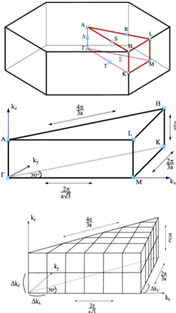
the wave vector k. The specific band label v 共c兲 represents filled共unfilled兲 bands, where for the clean cold semiconduc-tors, the band occupation factors are taken as either one or zero. The volume integration in Eq.共1兲 is over the first Bril-louin zone共BZ兲 which can be reduced to the irreducible BZ using the symmetry relations of the BZ共see, Fig.2兲.
The Dirac delta term in Eq.共1兲 automatically reduces the volume integration to a surface formed by the k points which allow direct 共vertical兲 transitions from a filled state to an unfilled state with an energy difference corresponding to the chosen photon energy. Such surface integrations routinely appear in the density of states, effective mass and response function calculations.27 They can be efficiently calculated
numerically using the Lehmann-Taut method.28 This tech-nique has also been shown to work for the second-order non-linear optical response function29 and also for the full band
phonon scattering rate calculation.22 In this work, for the
required accuracy, we divide the irreducible BZ into a mesh of 40⫻40⫻40 along the basal plane and the c-axis direc-tions共see, Fig.2兲. In Fig.3, we show the imaginary part of
the optical dielectric function for the intrinsic共i.e., undoped兲 InN and GaN. The ordinary tensor component which corre-sponds to the electric field parallel to basal plane of the hex-agonal crystal共i.e., in-plane兲 polarization is shown. For GaN, we observe a discrepancy between the theoretical and experimental31 values close to the band edge. On the other
hand, our theoretical result for InN matches well with the rigorous first-principles studies,32,33 and also in reasonable
agreement with the experiment.30
Another physical mechanism that accompanies band-filling is the BGR due to many-body interactions among the carriers.34In highly n-doped InN samples it is observed that
this partially cancels the Burstein-Moss effect.7The
electron-electron and electron-electron-ion contributions within the random phase approximation are given in Gaussian units by7,34
FIG. 1. 共Color online兲 The empirical pseudopotential band structures for InN共solid兲 and GaN 共dashed兲 used in this work.
FIG. 2. 共Color online兲 Schematic 共not to scale兲 of the Brillouin zone of the wurtzite structure 共top兲, its irreducible Brillouin zone 共middle兲, and its tessellation 共bottom兲; each volume is further di-vided into tetrahedra共not shown兲. a and c are the lattice constants in the basal plane and perpendicular directions, respectively.
⌬Ee−e= − 2e2kF ⑀s −e 2k TF 2⑀s
冋
1 − 4 arctan冉
kF kTF冊
册
, 共2兲 ⌬Ee−i= − 4e2N ⑀saBⴱkTF 3 , 共3兲where N is the electron 共ion兲 density and ⑀s is the static
permittivity for which we use the experimental value of 9.5 共15.3兲 for GaN 共InN兲.35,36 k
F=共32N兲1/3 and kTF
= 2
冑
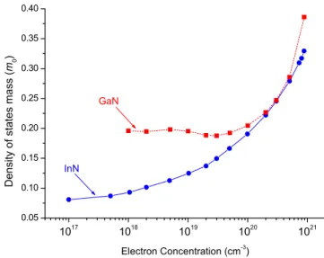
kF/共aBⴱ兲 are, respectively, the Fermi and Thomas-Fermiwave numbers, aBⴱ= 0.529⑀sm0/mⴱ is the effective Bohr ra-dius in Å, mⴱ is the conduction band effective mass. The latter quantity rapidly deviates with increase of energy from its band edge value, especially in the case of InN. Therefore, in these expressions we use an energy-dependent density of states effective mass value corresponding to the level of band-filling. Figure 4 shows for the conduction band these values used in this work for InN and GaN. The curve for InN is taken from the first-principles results.24 For GaN, it has
been computed using the same Lehmann-Taut method, but with a finer grid than used above, such as 60⫻60⫻60 or denser. In the case of photoexcitation which we consider for InN, actually we have a two-component quantum system 共i.e., electron and hole gases兲. In the interests of simplicity, we adapt Eq. 共2兲 by replacing the electron effective mass with the reduced electron-hole effective mass, eh given by eh −1 = me −1 + mh −1
where me and mh are the energy-dependent
electron and hole effective masses, respectively. The latter is almost constant for the densities dealt in this work and there-fore is taken to be 0.84m0for InN.
Having determined the imaginary dielectric function of a semiconductor with partially filled band共s兲, subject to BGR, the next aim is to compute their effect on the refractive in-dex. Their interrelation is established by the causality prin-ciple which has to be satisfied by any physical response function.37 In mathematical terms, this is governed by the
Kramers-Kronig relation; for the real part, the corresponding
expression, suppressing the Cartesian indices is given by
Re兵⑀共兲其 = 1 + 2 P
冕
0⬁
⬘
Im兵⑀共⬘
兲其
⬘
2−2 d⬘
. 共4兲 Computationally, it requires the knowledge of the imaginary part of the dielectric function for all energies; we have veri-fied the convergence of our results by including 60 bands and accounting for the higher energy behavior 共above 30 eV兲 analytically with a 1/2fall off.Based on the mechanisms described above, carrier injec-tion essentially leads to a change in the refractive index. Another significant contribution to the refractive index change is caused by the plasma absorption of the free carri-ers: electrons in the conduction band for the n-doped case or the electrons and holes for the photoexcited case. Its resultant contribution can be expressed in convenient units as15
⌬nplasma= −6.9⫻ 10 −22
n0mrⴱ
N关cm−3兴
E2关eV兴 , 共5兲 where n0is the refractive index of the intrinsic semiconduc-tor, E关eV兴 is the energy in eV, N关cm−3兴 is the free-carrier density in cm−3and m
r
ⴱis the effective mass in units of m 0; in the photoexcited case, for the latter two we use the electron-hole density and the effective mass共eh兲, respectively.
III. RESULTS
A. n-doped case in InN and GaN
We first start with the n-doped case which is quite easily achieved 共sometimes even unintentionally兲 in InN and GaN and, we explore the filling of the conduction band by elec-trons fully ionized from their dopants. The electron concen-trations up to about 7⫻1020 cm−3 共9⫻1020 cm−3兲 are con-sidered marking the threshold beyond which the next higher conduction band starts to be filled for InN 共GaN兲. Figure5
FIG. 3. 共Color online兲 Imaginary part of the in-plane optical dielectric function for the intrinsic InN and GaN, comparing our theoretical 共solid兲 results with the experimental 共dashed兲 data of Refs.30and31.
FIG. 4. 共Color online兲 The density-of-states effective mass variation as a function of band-filling for the conduction band elec-trons in InN and GaN. The latter is computed in this work, whereas the former is taken from Ref.24.
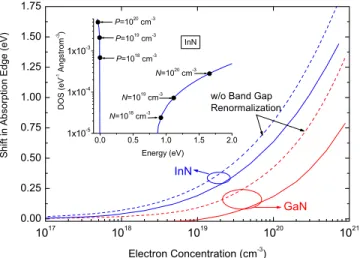
shows the shift in the absorption edge due to Pauli blocking of the filled portions of the lowest conduction band. A marked contrast revealed with this plot is that the absorption edge shift in InN is much more significant compared to GaN. The disparity between the two materials’ conduction band edge density of state behavior plays a role here. While in InN the band-filling effect is quite strong, in the case of GaN this becomes smaller which is moreover effectively canceled by the BGR.
Yoshikawa et al. have used temperature-dependent photo-luminescence spectroscopy to separate BGR and band-filling effects in Si doped GaN.38 Figure6 illustrates the
compari-son of our n-doped GaN results with this work for the re-duced band gap, i.e., due to BGR, as well as for the optical gap which corresponds to the absorption edge including the
BGR and Burstein-Moss effects. The dashed line is the fitted expression, −4.72⫻10−8n1/3 eV offered by Yoshikawa et al. for the former. Very recently Schenk et al. relying on band edge luminescence peak and the line shape information have extracted an expression given by −2.6⫻10−8n1/3 eV for the BGR in n-doped GaN.39While our result closely agrees with
the Yoshikawa data, Schenk’s expression is in disagreement with these. In Fig.6, also a much more elaborate theoretical analysis for the BGR is shown which however deviates from the rest of these results.40We believe that further studies are required to reach to a consensus over the BGR expression for GaN. The situation is more harmonious for InN. The com-parison of our computed absorption shift for InN with the measurements and calculation from Wu et al.,8together with
other data mentioned in that work41–43is provided in Fig.7; it shows the overall agreement of our results with the litera-ture.
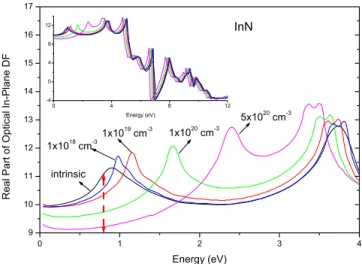
The conduction band filling and the associated BGR di-rectly affect the imaginary part of the dielectric functions through the shift in the absorption edge deeper into the con-duction band. This is illustrated for the ordinary components 共i.e., the electric field lying on the crystal basal plane兲 for different electron concentrations in Figs.8and9for InN and GaN, respectively. It can be noticed for both cases, especially for larger dopings, that there is a nonzero absorption below the absorption edge, even down to zero energy. This is due to intraband absorption within the conduction band 共see the upper inset in Fig.8兲. The same behavior also appears in the measured InN samples.8
The real parts of the dielectric functions are obtained from the imaginary parts using the Kramers-Kronig relation in Eq. 共4兲. The results are shown in Figs. 10 and 11 for InN and GaN, respectively. First of all, the real part of dielectric func-tion of InN is more sensitive to n-type doping. Furthermore, for low energies, the shifts are in opposite directions for InN and GaN, so that as the electron concentration increases, the permittivity decreases for InN, whereas it increases for GaN.
FIG. 5.共Color online兲 The shift in the absorption edge by n-type doping for GaN and InN due to conduction band filling without 共dashed兲 and with 共solid兲 BGR accounted. The inset shows the den-sity of states共DOS兲 for InN together with the band-filling levels on the valence and conduction bands in the absence of BGR.
FIG. 6.共Color online兲 The comparison for the n-doped GaN, the reduced gap and the optical gap values共see text兲 with Yoshikawa et
al.共Ref.38兲, Schenk et al. 共Ref.39兲, and Persson et al. 共Ref.40兲. The band gap of intrinsic GaN is taken as 3.5 eV.
FIG. 7. 共Color online兲 The comparison of measured and calcu-lated shifts in the absorption edge in InN with the calculation and measurements from Wu 共Ref. 8兲, together with other data men-tioned in that work: Haddad 共Ref. 43兲, Inushima 共Ref. 42兲, and Tyagai共Ref.41兲.
Note that these are only the electronic contributions to polar-ization as Eq.共1兲 does not include the ionic degrees of free-dom. Nevertheless the ions do not directly play a role in the change in the refractive index which is focus of this work. As mentioned in the Theory section, one should also add the free-carrier plasma contribution to the refractive index 关see, Eq. 共5兲兴. This is separately shown in Fig. 12 which always has a negative contribution, and兩⌬nplasma兩 decreases as 1/E2 with energy E.
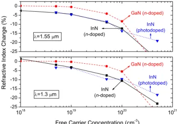
The overall change in the refractive index, including all of the effects mentioned so far is shown in Fig.13. Because of their technological importance, it is evaluated at the two fiber-optic communication wavelengths of 1.55 and 1.3 m which correspond to energies of 0.8 and 0.954 eV, respec-tively; the former is marked with dashed vertical arrows in Figs.10and11. It can be observed that the refractive index change due to n-type doping is much higher in InN
com-pared to GaN for both wavelengths. There are several rea-sons behind this outcome. First of all there is a cancellation that occurs for GaN; as shown in Fig. 5, BGR very effec-tively cancels the Burstein-Moss shift up to a density of 1019 cm−3. The lack of such a cancellation in InN is because of the very strong band-filling effect as a result of small density of states of InN close to conduction band edge, see the inset in Fig.5. Furthermore, contrary to the case in InN, the refractive index change in GaN due to band filling is positive up to the ultraviolet. This is canceled by the negative plasma contribution关cf., Eq. 共5兲兴, which actually dominates beyond a density of 1019 cm−3 in GaN and 1020 cm−3 in InN.
Note that at the 1.3 m wavelength the intrinsic as well as doped InN display substantial interband absorption 共see, Fig.8兲, hence, in Fig.13we used the following
generaliza-FIG. 8. 共Color online兲 The calculated imaginary part of the in-plane dielectric function 共DF兲 of InN for different n-type doping densities. Lower inset shows the same graph for a wider energy scale. Upper inset indicates the responsible intraconduction band transitions for the low energy part of the spectra.
FIG. 9. 共Color online兲 The calculated imaginary part of the in-plane dielectric function of GaN for different n-type doping densi-ties. Inset shows the same graph for a wider energy scale.
FIG. 10. 共Color online兲 The calculated real part of the in-plane electronic dielectric function of InN for different n-type doping densities. The vertical red arrow marks the 0.8 eV共1.55 m兲 value. Inset shows the same graph for a wider energy scale.
FIG. 11. 共Color online兲 The calculated real part of the in-plane electronic dielectric function of GaN for different n-type doping densities. The vertical red arrow marks the 0.8 eV共1.55 m兲 value. Inset shows the same graph for a wider energy scale.
tion of the refractive index in the presence of loss:37
n =
冑
冑
Re兵⑀其2+ Im兵⑀其2+ Re兵⑀其
2 . 共6兲
Because of this loss, 1.3 m case shows an overall reduc-tion in the refractive index change compared to 1.55 m wavelength. As another curious point, the n-doped InN curve in the bottom panel of Fig. 13 starts from a positive value which requires an explanation. Due to the absorption in the 1.3 m wavelength, the refractive index also peaks around the 0.95 eV range, particularly for the 1018 cm−3density共cf. Fig.10兲. Hence, the n-doped InN curve in Fig.13becomes positive for this density as its refractive index exceeds that of
the intrinsic sample. Even though the band-filling and plasma contributions try to reduce it, they are not as effective at this density.
B. Photoexcited case in InN
We would like to compare the pronounced refractive in-dex change in n-doped InN with the case where both elec-trons and holes are present. Since introducing holes with p-type doping is still a major technical challenge in InN,1we consider photodoping44where equal density of electrons and
holes are generated by a strong photoexcitation. We further assume that these photocarriers quickly thermalize to their respective band edges and attain a degenerate quasiequilib-rium distribution. Since the electron-hole pairs will eventu-ally recombine within a time scale of 300–400 ps,45the
qua-sicontinuous optical excitation should replenish this in order to sustain the assumed steady-state carrier distribution. The associated quasi-Fermi levels for different electron-hole den-sities are marked in the inset of Fig.5which clearly indicates that the contribution of the holes to the Burstein-Moss effect is negligible. In Fig. 14 we show the imaginary dielectric function at several electron-hole densities. Compared to the n-doped case in Fig.8, we observe two new features around 0 and 0.94 eV which are caused by the intravalence band transitions: the former is due to very low energy transitions at the valence band maximum共left inset in Fig.14兲, whereas the latter is the result of the⌫5v→⌫6vtransition共right inset in Fig. 14兲. It is the latter that makes a significant impact around 1.55 m 共0.8 eV兲 and even more so at the 1.3 m wavelength 共0.954 eV兲. Therefore, we would like to assert that our band structure agrees quite well with the other first-principle studies25,32 which report the value 0.9 eV with the
quasiparticle correction for the ⌫5v→⌫6v transition. As ob-served from Fig. 14, these new intravalence band channels refill the part of the spectra cleared by the Pauli blocking, undoing the Burstein-Moss effect. Also we can observe from
FIG. 12. 共Color online兲 The comparison of the free-carrier-induced refractive index change, i.e., plasma contribution,关see, Eq. 共5兲兴 for two different n-type doping densities for InN and GaN. The photoexcited N = P = 1019 cm−3bipolar case in InN is also included.
FIG. 13. 共Color online兲 The percentage refractive index change with respect to intrinsic共i.e., no free carrier兲 case for InN and GaN. All effects considered in this work are included, i.e., band-filling, BGR, and plasma contributions. Top panel shows the 1.55 m wavelength 共0.8 eV兲 and the bottom panel corresponds to the 1.3 m wavelength 共0.954 eV兲. See text, for the explanation of why n-doped InN curve in the bottom panel starts from a positive value. The lines are to guide the eyes.
FIG. 14. 共Color online兲 The calculated imaginary part of the in-plane dielectric function of InN for different electron-hole popu-lations forming degenerate quasiequilibrium distributions. Insets show the intravalence band transitions that give rise to the new absorption channels around 0 eV共left兲 and 0.94 eV 共right兲.
within the independent particle 共i.e., random phase兲 approximation,46 and as such, it neglects the excitonic
ef-fects. In the case of intrinsic InN dielectric function, it has been shown by Furthmüller et al. that, apart from small shifts in the energy positions, these excitonic effects are respon-sible for the enhancement of some of the peaks in the spec-tra, predominantly close to the band edge, while the general shape remaining as unaffected.32 Furthermore, in the
pres-ence of high concentration of free carriers, as considered in this work, the excitonic effects get perfectly screened. The transition from bound excitonic state to free electron-hole plasma takes place at the Mott critical density.37If we apply
its estimate from Ref. 15, we get about 5⫻1016 and 5 ⫻1018 cm−3 for InN and GaN, respectively. Above these values, excitons will dissociate which is easily met for the density range of this study.
On the BGR, there are other theoretical estimations, such as the plasmon-pole47 and the Vashishta-Kalia48 models. However, we observed that when contrasted with the existing experimental data on GaN共Ref.49兲 and InN,50the employed
Berggren-Sernelius expression34in this and recent studies7,8
outperforms these other models in the relevant high density range of this study. From a formal point of view, there exist more rigorous many-body approaches which incorporate ex-citons, BGR and band-filling effects in the same level, how-ever, their formidable computational cost leads to a trade off with a simplistic effective mass band structure.51
Furthermore, we should mention that the employed Berggren-Sernelius expression assumes a cubic crystal with parabolic bands.34 These simplifications have been avoided
by Persson and co-workers who have incorporated the electron-phonon contribution as well.40 Their framework is
particularly better suited for handling the BGR under photo-excitation where both electron- and hole-gas many-body contributions can be individually included. However, as we stated previously, in the photoexcited case we still use the Berggren-Sernelius expression but with the reduced electron-hole effective mass. Essentially, the same discussion also ap-plies for the plasma contribution in Eq. 共5兲.
Compared to the available ab initio results for InN,2,24,25,32our band structure is in good overall agreement.
Nevertheless, there remain further discrepancies of most of these theoretical results from the experimental data. First of all, due to the fact that our computational band gap of 0.85 eV for InN is somewhat higher than the experimentally
es-low as 7.5 to 15 meV which indicates that these features are anchored to just below the band gap.54
Being intended as a bulk study, this work neglects any surface effects, the most important of which is the surface charge accumulation causing built-in electric field and band bending.55,56 In this regard, it has been mentioned by
Kudrawiec et al. that for n-type InN layer since the region of strong band bending is the surface electron accumulation layer, it will not affect absorptionlike techniques such as pho-toreflectance spectroscopy due to band filling of the conduc-tion band.57Another effect discarded in this study is the ther-mal smearing of the degenerate carrier statistics. As a possible follow up of this work it can be readily included, nevertheless we do not expect any marked deviations. Even though the quasi-Fermi level shift in the valence band is of the same order as the thermal energy共cf., inset of Fig.5兲, as shown above, the main effect is driven by the Fermi level shift in the conduction band, which by far outweighs any thermal energy well up to room temperature for the carrier densities important for this work. Stemming from these ide-alizations, our main results in Fig. 13 should be taken as upper bounds. The list of these simplifications also suggests possible improvements of this work.
To harness the carrier-induced refractive index change such as in phase modulators, the associated losses need to be minimized. In this respect, the narrow 0.64 eV band gap of InN becomes undesirable for the 1.55 and 1.3 m
applica-TABLE I. Fitted values for the constants in the pseudopotential form factors Vsand Va; see Eqs.共1兲 and 共2兲. Other parameters used in the EPM are also listed, where a and c are the lattice constants in the hexagonal plane and along the c axis, respectively, u is the wurtzite internal structural parameter, and Emaxdenotes the radius of the energy sphere used for the reciprocal lattice vectors.
s1= 0.261905 a1= −0.411320 s2= 0.232300 a2= 0.176416 s3= −2.726784 a3= 1.441420 s4= 0.973335 a4= 0.915637 s5= 2.414422 a5= 2.595997 a = 3.544 Å c = 5.716472 Å u = 0.379 Emax= 12.5 Ry
toward the choice of indium-rich alloys.
V. CONCLUSIONS
We have shown that based on a full band theoretical analysis, under n-type doping, InN and GaN should display different dielectric characteristics. The absorption edge shift is masked in GaN, whereas it is highly pronounced in InN. For energies below 1 eV, the corresponding shifts in the real parts of the dielectric function for InN and GaN are in op-posite directions. The free-carrier plasma contribution to re-fractive index becomes dominant above 1020 cm−3 for the case of InN. At a wavelength of 1.55 m, we predict more than 4% of change in the refractive index for InN for a dop-ing of 1019 cm−3. Under optical pumping which fills the con-duction and valence band edges with electrons and holes of equal density, the refractive index is not further affected by the presence of the holes. However, its major consequence is the increased intravalence band absorption as a result of⌫5v →⌫6
v
transition. Beyond a hole density of 1019 cm−3, this affects 1.3 to 1.55 m wavelengths. We believe that this wide tunability of the index of refraction in InN by the con-duction band electrons is technologically important for appli-cations such as optical phase modulators. In the presence of holes, the valence band absorption needs to be taken into account, such as in the design of InN-based lasers for fiber-optics applications. Our findings suggest that the alloy
com-In the light of recent experimental and first-principles studies on wurtzite InN, we have expressed the local empiri-cal pseudopotential method 共EPM兲 form factors using the following functional form,
Vs共q兲 = 共s1q3+ s2q2+ s3兲exp共− s4qs5兲, 共A1兲 Va共q兲 = 共a1q2+ a2q + a3兲exp共− a4qa5兲, 共A2兲 where Vs and Vaare the symmetric and antisymmetric form
factors in Rydbergs, q is the wave number in units of 2/a with a being the lattice constant in the hexagonal plane, and si, ai共i=1, ... ,5兲 are the fitting parameters which are listed
in Table I.
The nonlocal part of the pseudopotential is based on the classical work of Chelikowsky and Cohen,58 with the
plane-wave matrix elements being given by
VNL共Kជ,Kជ 兲 =
⬘
4 ⍀a兺
l,i Al i共E兲共2l + 1兲P l关cos共KK⬘兲兴Si共Kជ − Kជ⬘
兲Fl i共K,K⬘
兲, 共A3兲where Si共q兲 is the structure factor58for the atomic species i,
and Pl共x兲 is the Legendre polynomial corresponding to
angular-momentum channel l,⍀ais the atomic volume共i.e.,
primitive cell volume divided by number of atoms兲, Kជ= kជ + Gជ, Kជ
⬘
= kជ+ Gជ⬘
, and Fl共K,K⬘
兲 =冦
R3 2兵关jl共KR兲兴 2− j l−1共KR兲jl+1共KR兲其, K = K⬘
, R2 K2− K⬘
2关Kjl+1共KR兲jl共K⬘
R兲 − K⬘
jl+1共K⬘
R兲jl共KR兲兴, K ⫽ K⬘
冧
共A4兲here, jl共x兲 is the spherical Bessel function, R is 共momentum-dependent兲 well width. For InN, we treat the
共2002兲.
8J. Wu, W. Walukiewicz, S. X. Li, R. Armitage, J. C. Ho, E. R.
Weber, E. E. Haller, H. Lu, W. J. Schaff, A. Barcz, and R. Jakiela,Appl. Phys. Lett. 84, 2805共2004兲.
9J.-F. Vinchant, J. A. Cavaillès, M. Erman, P. Jarry, and M.
Renaud,J. Lightwave Technol. 10, 63共1992兲.
10D. G. Deppe, N. D. Gerrard, C. J. Pinzone, R. D. Dupuis, and E.
F. Schubert,Appl. Phys. Lett. 56, 315共1990兲.
11J.-P. Weber,IEEE J. Quantum Electron. 30, 1801共1994兲. 12P. A. Kirkby, A. R. Goodwin, G. H. B. Thompson, and P. R.
Selway,IEEE J. Quantum Electron. 13, 705共1977兲.
13A. Olsson and C. L. Tang,Appl. Phys. Lett. 39, 24共1981兲. 14N. K. Dutta, N. A. Olsson, and W. T. Tsang,Appl. Phys. Lett.
45, 836共1984兲.
15B. R. Bennett, R. A. Soref, and J. A. Del Alamo,IEEE J.
Quan-tum Electron. 26, 113共1990兲.
16L. Chusseau, P. Martin, C. Brasseur, C. Alibert, P. Hervé, P.
Arguel, and F. Lozes-Dupuy,Appl. Phys. Lett. 69, 3054共1996兲.
17P. P. Paskov,J. Appl. Phys. 81, 1890共1997兲.
18W. W. Chow, H. Amano, and I. Akasaki, Appl. Phys. Lett. 76,
1647共2000兲.
19U. T. Schwarz, E. Sturm, W. Wegscheider, V. Kümmler, A. Lell,
and V. Härle,Appl. Phys. Lett. 83, 4095共2003兲.
20M. Röwe, P. Michler, J. Gutowski, V. Kümmler, A. Lell, and V.
Härle,Phys. Status Solidi A 200, 135共2003兲.
21C. Bulutay and N. A. Zakhleniuk,Phys. Status Solidi C 5, 511
共2008兲.
22C. Bulutay, B. K. Ridley, and N. A. Zakhleniuk,Phys. Rev. B 62, 15754共2000兲.
23C. Bulutay and B. K. Ridley,Superlattices Microstruct. 36, 465
共2004兲.
24P. Carrier and S.-H. Wei,J. Appl. Phys. 97, 033707共2005兲. 25D. Bagayoko and L. Franklin,J. Appl. Phys. 97, 123708共2005兲. 26J. L. P. Hughes and J. E. Sipe,Phys. Rev. B 53, 10751共1996兲. 27R. M. Martin, Electronic Structure共Cambridge University Press,
Cambridge, England, 2004兲.
28G. Lehmann and M. Taut,Phys. Status Solidi B 54, 469共1972兲. 29D. J. Moss, J. E. Sipe, and H. M. van Driel,Phys. Rev. B 36,
1153共1987兲.
30R. Goldhahn, A. T. Winzer, V. Cimalla, O. Ambacher, C. Cobet,
W. Richter, N. Esser, J. Furthmüller, F. Bechstedt, H. Lu, and W. J. Schaff,Superlattices Microstruct. 36, 591共2004兲.
31L. X. Benedict, T. Wethkamp, K. Wilmers, C. Cobet, N. Esser, E.
L. Shirley, W. Richter, and M. Cardona,Solid State Commun.
112, 129共1999兲.
38M. Yoshikawa, M. Kunzer, J. Wagner, H. Obloh, P. Schlotter, R.
Schmidt, N. Herres, and U. Kaufmann,J. Appl. Phys. 86, 4400 共1999兲.
39H. D. P. Schenk, S. I. Borenstain, A. Berezin, A. Schön, E.
Cheifetz, S. Khatsevich, and D. H. Rich, J. Appl. Phys. 103, 103502共2008兲.
40C. Persson, B. E. Sernelius, A. Ferreira da Silva, C. Moyseś
Araújo, R. Ahuja, and B. Johansson, J. Appl. Phys. 92, 3207 共2002兲.
41V. A. Tyagai, A. M. Evstigneev, A. N. Krasiko, A. F. Andreeva,
and V. Ya. Malakhov, Sov. Phys. Semicond. 11, 1257共1977兲.
42T. Inushima, T. Yaguchi, A. Nagase, A. Iso, and T. Shiraishi,
Inst. Phys. Conf. Ser. 142, 971共1996兲; T. Inushima, T. Shiraishi, and V. Yu. Davydov,Solid State Commun. 110, 491共1999兲.
43D. B. Haddad, J. S. Thakur, V. M. Naik, G. W. Auner, R. Naik,
and L. E. Wenger, Mater. Res. Soc. Symp. Proc. 743, L11.22 共2002兲.
44There exists a somewhat different use of the “photodoping”
ter-minology to describe the dissolution of metals, such as Ag or Cu, into chalcogenide glasses under an illumination. However, this is more appropriately termed as photodissolution共Ref.59兲.
45F. Chen, A. N. Cartwright, H. Lu, and W. J. Schaff,Appl. Phys.
Lett. 83, 4984共2003兲.
46H. Ehrenreich and M. H. Cohen,Phys. Rev. 115, 786共1959兲. 47H. Haug and S. W. Koch,Phys. Rev. A 39, 1887共1989兲. 48P. Vashishta and R. K. Kalia,Phys. Rev. B 25, 6492共1982兲. 49T. Nagai, T. J. Inagaki, and Y. Kanemitsu,Appl. Phys. Lett. 84,
1284共2004兲.
50P. Schley, R. Goldhahn, A. T. Winzer, G. Gobsch, V. Cimalla, O.
Ambacher, H. Lu, W. J. Schaff, M. Kurouchi, Y. Nanishi, M. Rakel, C. Cobet, and N. Esser, Phys. Rev. B 75, 205204 共2007兲.
51J. P. Löwenau, S. Schmitt-Rink, and H. Haug, Phys. Rev. Lett. 49, 1511共1982兲; J. P. Löwenau, F. M. Reich, and E. Gornik, Phys. Rev. B 51, 4159共1995兲.
52W. Z. Shen, L. F. Jiang, H. F. Yang, F. Y. Meng, H. Ogawa, and
Q. X. Guo,Appl. Phys. Lett. 80, 2063共2002兲.
53B. Arnaudov, T. Paskova, P. P. Paskov, B. Magnusson, E.
Val-cheva, B. Monemar, H. Lu, W. J. Schaff, H. Amano, and I. Akasaki,Phys. Rev. B 69, 115216共2004兲.
54A. Klochikhin, V. Davydov, V. Emtsev, A. Sakharov, V.
Kapi-tonov, B. Andreev, H. Lu, and W. J. Schaff,Phys. Status Solidi A 203, 50共2006兲.
55H. Lu, W. J. Schaff, L. F. Eastman, and C. E. Stutz,Appl. Phys.