ENVIRONMENTAL FRIENDLY
InP/ZnS NANOCRYSTALS
A THESIS
SUBMITTED TO THE DEPARTMENT OF MATERIALS SCIENCE AND NANOTECHNOLOGY
AND THE GRADUATE SCHOOL OF ENGINEERING AND SCIENCE OF BILKENT UNIVERSITY
IN PARTIAL FULLFILMENT OF THE REQUIREMENTS FOR THE DEGREE OF
MASTER OF SCIENCE
By
Yasemin COŞKUN
May 2012
ii
I certify that I have read this thesis and that in my opinion it is fully adequate, in scope and in quality, as a thesis for the degree of Master of Science.
Assoc. Prof. Hilmi Volkan Demir (Supervisor)
I certify that I have read this thesis and that in my opinion it is fully adequate, in scope and in quality, as a thesis for the degree of Master of Science.
Assoc. Prof. Dönüş Tuncel
I certify that I have read this thesis and that in my opinion it is fully adequate, in scope and in quality, as a thesis for the degree of Master of Science.
Prof. Oğuz Gülseren
Approved for the Graduate School of Engineering and Sciences:
Prof. Levent Onural
iii
ABSTRACT
ENVIRONMENTAL FRIENDLY InP/ZnS NANOCRYSTALS
Yasemin Coşkun
M.S. in Materials Science and Nanotechnology
Supervisor: Assoc. Prof. Hilmi Volkan Demir
May 2012
Semiconductor nanocrystals are nanometer scale fluorescent crystallites with tunable optical properties, which can be controlled by the material composition and particle size. They can be prepared using various synthesis techniques and find applications in many different areas ranging from life sciences to electronics. In this thesis, indium phosphide based nanocrystals are studied for LED applications. The thesis research work focuses on the colloidal synthesis method and material characterization of these nanocrystals. Using one pot synthesis method, the indium phosphide/zinc sulfide (InP/ZnS) core/shell nanocrystal structures are synthesized. This synthesis technique allows for a reproducible and tunable preparation method. The material characterization techniques used in this thesis include UV-Vis spectroscopy, photoluminescence spectroscopy, transmission electron microscopy (TEM), X-ray diffraction, X-ray photoelectron spectroscopy (XPS), inductively coupled plasma-mass spectrometry (ICP-MS), and Zeta Sizer (or DLS). These properties make InP/ZnS nanocrystals comparable to their cadmium (Cd) containing counterparts with respect to their optical properties, and InP/ZnS nanocrystals offer the potential to replace them because of environmental concerns in LED applications.
iv
ÖZET
ÇEVRE DOSTU InP/ZnS NANOKRİSTALLER
Yasemin Coşkun
Malzeme Bilimi ve Nanoteknoloji Bölümü Yüksek Lisans
Tez Yöneticisi: Doç. Dr. Hilmi Volkan Demir
Mayıs 2012
Yarı iletken nanokristaller nanometre boyutunda, optik özellikleri materyal kompozisyonu ve parçacık boyutu kontrol edilerek ayarlanabilen floresan kristalciklerdir. Yarı iletken nanokristaller çeşitli sentez teknikleri kullanılarak hazırlanabilirler ve biyolojik bilimlerden elektroniğe kadar bir çok farklı alanda uygulama bulurlar. Bu tez içerisinde LED uygulamaları için indiyum fosfat tabanlı nanokristaller çalışıldı. Bu tezin araştırma çalışmaları bu nanokristallerin koloidal sentez metodu ve materyal karakterizasyonlarına odaklanmıştır. Tek kap sentez metodu kullanılarak, indiyum fosfat/çinko sülfat (InP/ZnS) çekirdek/kabuk nanokristal yapıları sentezlenmiştir. Bu sentez tekniği tekrarlanabilir ve ayarlanabilir bir hazırlama metodu sağlamaktadır. Tezde çalışılan malzeme karakterizasyon teknikleri UV-Vis spektroskopi, fotoluminesans spektroskopisi, geçirimli elektron mikroskopisi (TEM), x-ışını kırınımı, x-ışını fotoelektron spektroskopisi (XPS), etkileşik çiftlenmiş plazma (ICP-MS) ve Zeta boyut ayırıcını (ya da DLS) içerir. Bu özellikler InP/ZnS nanokristalleri kadmiyum (Cd) içeren rakipleriyle optik özellikleri açısından karşılaştırılabilir hale getirmektedir ve çevresel sebeplerle InP/ZnS nanokristaller LED uygulamalarında Cd içeren nanokristaller yerine kullanılmaktadır.
v
vi
ACKNOWLEDGEMENTS
First of all, I would like to thank my supervisor Prof. Hilmi Volkan Demir for his invaluable guidance, encouragement and helpful suggestions during my research in Bilkent University.
I would also like to thank my MS thesis committee members Prof. Dönüş Tuncel and Prof. Oğuz Gülseren.
I would like to thank and acknowledge Dr. Evren Mutlugün, Dr. Vijay Kumar Sharma and Cüneyt Eroğlu for sharing their knowledge and giving me their support during my thesis work.
I would also like to thank all members of Demir Group: Özgün Akyüz, Emre Ünal, Dr. Nihan Kosku Perkgöz, Dr. Urartu Ö. Şeker, Dr. Pedro L. Hernandez, Emre Sarı, Can Uran, Aydan Yeltik, Talha Erdem, Burak Güzeltürk, Sayim Gökyar, Kıvanç Güngör, Ahmet Fatih Cihan, Shahab Akhavan, Yusuf Keleştemur, Togay Amirahmadov, Ozan Yerli, Veli Tayfun Kılıç, İbrahim Akçalı and Halil Akçalı for their friendship.
I would like to thank all my family especially my precious siblings Süleyman Coşkun and Hanife Coşkun for their encouragement. I would like to thank my best friend Aylin Acun for her friendship and the wonderful times we spent together. I especially thank İlker Tezsevin for his support, patience and for many things he has done for me unconditionally.
Finally, I would like to express my deepest gratitude to my parents Galip Coşkun and Arife Coşkun for their constant support, patience and sincere love without any expectation.
vii
TABLE OF CONTENTS
ABSTRACT iii ÖZET iv ACKNOWLEDGEMENTS vi 1. INTRODUCTION 1 1.1. Nanomaterials 1 1.1.1. Classification of Nanocrystals 5 1.1.2. Synthesis of Nanocrystals 7 1.2. Material Characterization 8 1.2.1. UV-Vis-NIR Spectroscopy 9 1.2.2. Fluorescence Spectroscopy 101.2.3. Transmission Electron Microscopy (TEM) 11
1.2.4. Scanning Electron Microscopy (SEM) and Energy Dispersive X-ray
Spectroscopy (EDAX) 12
1.2.5. Inductively Coupled Plasma-Mass Spectrometry (ICP-MS) 12
1.2.6. X-Ray Photoelectron Spectroscopy (XPS) 13
1.2.7. Zeta Sizer: Dynamic Light Scattering (DLS) 15
1.2.8. X-Ray Diffraction (XRD) 17
1.3. Motivation of This Study 18
viii
2.1. Synthesis of Nanocrystals 19
2.1.1. Materials Used 20
2.1.2. First Synthesis Method 20
2.1.3. Second Synthesis Method 23
2.1.3.1. Core Synthesis 24
2.1.3.2. Shell Synthesis 25
2.2. Purification of Nanocrystals 27
3. NANOCRYSTAL MATERIAL CHARACTERIZATION AND APPLICATIONS 29
3.1. Elemental Study 30
3.2. Size Study 33
3.3. Crystal Structure Study 39
3.4. Core/Shell Study 42
3.5. Applications 49
4. CONCLUSIONS 54
BIBLIOGRAPHY 56
ix
LIST OF FIGURES
Figure 1.1.1. Unit cell of InP in zinc blende structure [1] 3
Figure 1.1.1.1. Electronic energy levels of some semiconductor materials in which CB and VB represents the conduction band and the valance band,
respectively [2] 6
Figure 1.1.1.2. Types of core/shell NCs depending on the energy-level
alignment [3] 6
Figure 1.2.3.1. Schematic representation of basic components of TEM [4] 11 Figure 1.2.6.1. Schematic representation of (a) photoionization process and
(b) Auger electrons [5] 14
Figure 1.2.7.1. Components of Zetasizer Nano series for DLS measurements
[6] 16
Figure 2.1.2.1. Photograph of glove box system 21
Figure 2.1.2.2. Our synthesis setup 22
Figure 2.1.2.3. Color change of the reaction solution during heating process: (a) at low temperatures (<40˚C), (b) at around 60˚C, and (c) at 300˚C 22 Figure 2.1.2.4. Absorption and photoluminescence spectra for three samples
of InP/ZnS NCs 23
Figure 2.1.3.2.1. Syringe pump used in the ZnS shell synthesis for the injection
of S source 26
Figure 2.2.1. Purified InP/ZnS core/shell NCs: (a) without UV excitation and (b)
under UV light 28
Figure 2.2.2. Photoluminescence spectra of purified InP/ZnS NCs emitting at (a) 625 nm as red, (b) 590 nm as orange, (c)555 nm as yellowish green, and (d)
x
Figure 3.1.1. EDAX results given for the selected areas (a) for the outside area
of InP core NCs and (b) for the sample detected by SEM 30
Figure 3.1.2. EDAX results given for the selected areas (a) for the outside area of InP/ZnS core/shell NCs and (b) for the sample detected by SEM 31
Figure 3.1.3. EDAX result of bue-emitting InP/ZnS NCs 32
Figure 3.1.4. ICP-MS results for InP core, InP/ZnS core/shell, and InP/ZnS
core/thicker shell: Selected row represents the amounts for In and Zn in ppb 32 Figure 3.2.1. Magnified TEM images of (a) InP core NC (with a diameter of 2 nm), (b) InP/ZnS core/shell NC (3.4 nm), and (c) InP/ZnS core/thicker shell NC
(4.2 nm) 33
Figure 3.2.2. Sketch of a core/shell NC structure 34
Figure 3.2.3. DLS size distribution for InP/ZnS NC samples (a) after the 1st purification and (b) after the 4th purification, along with their TEM images 38 Figure 3.3.1. XRD spectroscopy of InP core and InP/ZnS core/shell NCs with
their calculated lattice parameters 39
Figure 3.3.2. (a) TEM image (2 nm) and (b) selected area electron diffraction
pattern of InP core NCs 40
Figure 3.3.3. (a) TEM image (3 nm) and (b) selected area electron diffraction
pattern of InP/ZnS core/shell NCs 41
Figure 3.4.1. Absorption and PL spectra of the InP core and InP/ZnS core/shell
NCs 43
Figure 3.4.2. XPS survey data for InP core, InP/ZnS core/shell and InP/ZnS
thicker shell NCs 44
Figure 3.4.3. XPS survey showing indium peaks for InP core, InP/ZnS
core/shell and InP/ZnS thicker shell NCs 44
Figure 3.4.4. XPS results of In, P, Zn, S peaks for NC of InP core (Core), InP/ZnS core/shell (CS1) and InP/ZnS core/thicker shell (CS2) samples 45 Figure 3.4.5. Zn to In peak count ratio taken from XPS results for the InP core, InP/ZnS core/shell and InP/ZnS core/thicker shell NCs to be 0.2, 1.9, and 9.4 46 Figure 3.4.6. XPS results of phosphorus peaks for (a) InP core NCs, (b) InP/ZnS
core/shell NCs, and (c)InP/ZnS core/thicker shell NCs 47
xi
Figure 3.4.8. TEM image of InP/ZnS core/shell NC sample 48
Figure 3.4.9. TEM image of InP/ZnS core/thicker shell NC sample 49 Figure 3.5.1. Photographs of InP/ZnS NC-PMMA freestanding membrane films (dimensions of 2cm x 3cm) prepared with (a) red-emitting NCs, (b)
green-emitting NCs, and (c) blue green-emitting NCs 50
Figure 3.5.2. Normalized PL peaks for the thin films of green and red InP/ZnS
NCs mixed with PMMA 51
Figure 3.5.3. Normalized PL peaks for the thin films of green and red InP/ZnS
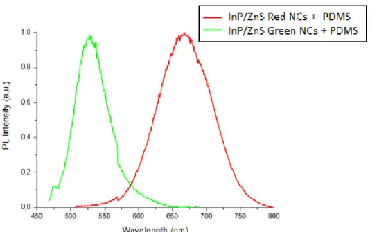
NCs mixed with PDMS 52
Figure 3.5.4. Photograph of a 51 cm x 51 cm InP/ZnS core/shell NC embedded membrane films under (a) room light, and (b) UV light [7] 52 Figure 3.5.5. Electroluminescence spectra of white LED using InP/ZnS
core/shell NCs membrane films applied on a blue LED chip. An exemplary
xii
LIST OF TABLES
Table 1.1.2.1. Material parameters of selected bulk semiconductors [8] 8
Table 2.1.3.1.1. Temperature variation study for InP core NCs 24 Table 3.2.1. Indium to zinc intensity ratio of InP/ZnS core/shell NCs and
InP/ZnS core/thicker shell NCs as found from XPS 36
Table 3.2.2. Radii found by TEM and XPS results 37
Table 3.3.1. Calculated lattice parameters by using TEM diffraction pattern
1
CHAPTER 1
INTRODUCTION
This thesis focuses on environmental friendly InP/ZnS core/shell nanocrystals (NCs) including their synthesis method, characterization and application examples. Firstly, a brief introduction is given in Chapter 1. Then, in Chapter 2, synthesis procedures are explained in detail with some illustrations. Subsequently, in Chapter 3, characterization studies and application examples are provided for elemental study, size study, crystal structure study, core/shell study, and applications.
1.1. Nanomaterials
Nanoscience has started to attract the world’s attention because of its potential impact on industry. Therefore, the emphasis on nanoscience grows stronger with each passing day. The area of nanoscience in the field of semiconductors is in principal the combination of different disciplines including materials science, chemistry, physics, engineering and biology. For the synthesis of developed nanoparticles, scientists have been working on different methods with different materials and using different routes [9].
Nanoparticles are the major class of nanomaterials that are quasi zero-dimensional. These particles have diameters of one to few hundred nanometers, and their optical
2
and electronic properties strongly depend on their sizes. Properties of small nanoparticles are different from those of large ones (larger than 20-50 nm), which have similar properties in their bulk structures. Nanoparticles can either be amorphous or crystalline, and crystalline nanoparticles are called as nanocrystals [10].
Nanocrystals, or nano-meter scale semiconductor crystallites, have been studied over the past two decades in order to understand the behaviour of semiconductor when they become small with diameters around from 1 to 10 nm [8, 11]. These materials are composed of an inorganic core, which consists of few hundred or few thousands of atoms, sometimes a shell surrounding the core, and an organic surfactant layer, or ligands, which prevent them from agglomeration [3, 8]. Because of having small size, the quantum confinement effect, which manifests itself as increasing bandgap with quantization of the energy states to further generated discrete levels, becomes observable, and its theoretical model is mainly based on the particle in a box model in quantum mechanics [12].
Many of the organically pasivated cores have some surface trap states, which act as non-radiative recombination centers for charge carriers, and this results in decreased quantum efficiency or quantum yield [3]. The best way to improve the case is surface passivation by means of a shell formation using a wider bandgap semiconductor. Core/shell nanocrystal systems exhibit better fluorescence with a better quantum yield and a better resistance against oxidization. Moreover, the choice of shell material can also help to tune the peak emission wavelength of the final NC structure.
Nanocrystal work has started in the early 1980s [13, 14]. However, semiconductor NCs were not fully understood till 1993 after when a remarkable progress was made on the semiconductor NC synthesis. Bawendi and his co-workers developed a novel synthesis method with a low size dispersion of 2-12 nm for Cd containing NCs [15].
3
Low size dispersion is an important parameter for NC work since the NC properties are strongly dependent on the size. Besides, the core/shell NCs have been started to be studied extensively because of their superior optical properties compared to their only core cases.
However, growing shells on core NCs is not an easy task but very critical for high efficiency. Both core and shell materials are required to crystallize in the same structure and, as a result, to have a small lattice mismatch [8]. Small lattice mismatch means close lattice constants for the core and shell materials. For the case of InP and ZnS core/shell materials, these constants are 5.87 and 5.41 Å, respectively, and their lattice mismatch is around 7%, which is acceptable [16]. The crystal structure of these materials is zinc blende, shown in Figure 1.1.1. Since both have the same crystal structure, ZnS also has the same unit cell, with Zn instead of In and S instead of P.
Figure 1.1.1. Unit cell of InP in zinc blende structure [1].
In history, the development of synthetic procedures for semiconductor NCs has started with Cd containing NCs as indicated earlier. Various NCs have been synthesized, including those in II-IV, III-V, and IV-VI depending on the group number of materials used for final NC structure. Some of these particles can be synthesized
4
in aqueous media [17, 18] but they can also be synthesized in different mediums like in ionic liquids [19], oil-water system [20], or in microemulsions [21].
In this thesis, the main focus is on Cd-free III-V nanophosphor core/shell NCs including InP/ZnS. III-V NCs are studied less extensively when compared to II-VI compounds, although NCs containing group III-nitrides and phosphide compounds are most generally referred to as greener NCs than those containing the elements like Cd, Pb, Hg or Te [22]. However, their synthesis methods are fewer and not so stable, which requires more work in this area. However, there are more studies recently reported due to environmental concerns and low acceptability of cadmium containing NCs in technological applications and life sciences [3, 23, 24].
Among Cd-free materials, mostly studied compounds in the literature are indium phosphide (InP) and indium aresenide (InAs) NCs, which have bulk band gap energies of 1.27 and 0.46 eV respectively. However, InAs also contains As which is Class B elements in terms of toxicity (whereas Class A contains Cd and Hg). Therefore, InP is the most promising candidate for environmental friendly NCs [25, 26]. They can offer a similar or even broader emission range, similar to their Cd containing counterparts without having intrinsic toxic property, whereas they exhibit poor optical properties typically, their PL emission full-width-half-maximum (FWHM) lies around 50-100 nm, and their quantum yield is relatively low . Cd-free type of NCs are first reported by Nozik and his colleagues and they observed strong band-edge emission for InP NCs [27, 28]. Then, Heath et al. reported the size-selective and surface passivated InP NC sytnhesis procedure in 1996. However, the quantum efficiency was still a problem, which was reported to be better for smaller NCs, having less than a 2% quantum yield [29]. Subsequently, some groups also worked on increasing efficincies of synthesized NCs, and Micic and Talapin obtained the efficiencies of 30-40% by photoassisted etching techniques. They obtained the highest efficiency level reported till then because they were able to remove the surface phosphorus atoms causing surface trap states [28, 30].
5
In order to obtain better properties and higher efficiencies, researchers started to grow shell on InP core NCs, although sometimes they can also make efficient InP/ZnS alloy structures [31]. First, Xie et al. proposed a new route for the growth of ZnS shell on InP core in 2007 and managed to synthesize high quality NCs [26]. Then, Li and Reiss developed a single step synthesis method depending on the difference in reactivity of the InP and ZnS precursors and they obtained a quantum yield up to 50-70% with high photostability [32]. They also used highly reactive precursors for the synthesized NCs to obtain higher quality, and they reached around 20% quantum yield for their prepared InP/ZnS core/shell NCs [22]. Moreover, Xu et al. proposed a fast synthesis method for InP/ZnS core/shell NCs covering the range of blue to near-infrared with a reported efficiency level of up to 60% [33].
Doping is another technique used for the synthesis of doped InP/ZnS NCs. Xie and Peng developed an efficient Cu-doped NCs with an efficiency level around 35-40% [34]. The main problem with all aqueous synthetic methods of InP/ZnS NCs is their large size dispersion of at least 15%. Because of this reason, additional methods such as size selective precipitation after preparation of these NCs gain importance for obtaining monodisperse NCs.
1.1.1. Classification of Nanocrystals
Core/shell NCs can be classified according to their relative position of bandgap energy levels. Figure 1.1.1.1. represents the electronic energy levels of some mostly using semiconductors.
6
Figure 1.1.1.1. Electronic energy levels of some semiconductor materials in which CB and VB represents the conduction band and the valance band, respectively [2].
According to the choice of the materials for the core and the shell, the core/shell NC structure can be named as type-I, type-II, and reverse type-I, as shown in Figure 1.1.1.2.
Figure 1.1.1.2. Types of core/shell NCs depending on the energy-level alignment [3].
In Figure 1.1.1.2, the upper and lower edges correspond to the position of the conduction and valance band edges, respectively. Also, the center figures show the core and the side figures indicate shell material. As can be understood from the figure, if the bandgap of the shell material is larger than that of the core, it belongs
7
to type-I and both electrons and holes are confined in the core. In the complimentary case, if the bandgap of the core material is larger than that of the shell, electrons and holes are either partially or completely confined in the shell. Finally, in type-II core/shell NCs, either the conduction or valance band edge of the shell material is smaller than that of the core, while the other is larger. In that case, electrons and holes are separated in different regions of the core/shell structure [3].
1.1.2. Synthesis of Nanocrystals
Semiconductor NCs can be synthesized by using wet chemistry [32, 35], molecular beam epitaxy (MBE) [36, 37], metal-organic chemical vapor deposition (MOCVD) [38], and organometallic vapor phase epitaxy (OMVPE) [39] methods. Using wet chemistry, colloidal NCs can be obtained.
In wet chemistry, stability of the NCs is an important issue and it is related to the presence of ligand shell. The ligands are adsorbed on the surface of NCs and prevent them from aggregation in solution. Ligands can provide stability both in aqueous medium and in organic medium. In aqueous medium, Coulomb interactions between the ligand species enable the necessary repulsive forces against attractive van der Waals forces between grains. On the other hand, in organic medium, the increase in solute concentration provides repulsive forces [10].
To increase the stability, the shell growth is the key point, but this needs to be epitaxial growth, which is required for the NCs to have better optical properties. Shell material should be carefully chosen with a small lattice mismatch to avoid trap states on the surface leading to low quantum yield. Also, appropriate shell precursors should be used in the synthesis and the precursors should possess high reactivity and selectivity so there will be no side reactions [3]. Table 1.1.2.1 represents some of the material parameters for mostly studied semiconductors.
8
Table 1.1.2.1. Material parameters of selected bulk semiconductors [8].
1.2. Material Characterization
Determination of the NC structure is another important point in a NC study. Some basic characterization techniques are used for the core and core/shell NCs including UV-Vis and photoluminescence spectroscopy. Additionally, transmission electron microscopy (TEM), X-ray diffraction, X-ray photoelectron spectroscopy (XPS), inductively coupled plasma-mass spectrometry (ICP-MS), and Zeta Sizer (or DLS) can be used for their characterization.
9
1.2.1. UV-Vis-NIR Spectroscopy
UV-Vis NIR spectroscopy is one of the essential techniques to determine optical properties of NC materials and used to detect the amount of light absorbed in them at different wavelengths. Ultraviolet (UV), visible, short-wave near-infrared, and long-wave near-infrared cover the ranges of 190-380 nm, 380-750 nm, 750-1100 nm, 1100-2500 nm, respectively. UV-Vis-NIR offers some different measurement modes; namely, scan (absorbance vs wavelength), time drive (absorbance vs time at specific wavelength), individual wavelength(s) (individual absorbance(s) at selected wavelength(s), chemometrics, and quantitative methods (concentration of analyte vs. absorbance), and kinetics (kinetic rates of reaction) mode [40]. In nanocrystals characterization, the scan mode is used to make quantum yield measurements. In spectroscopic measurements, Beer-Lambert law is commonly used for quantitative analysis since the relation is useful for detecting concentration of the sample in a specimen. Beer-Lambert law is given by
(1)
where T is the transmittance, I is the intensity of transmitted light, I0 is the intensity of incident light, is the molar extinction coefficient, c is the concentration, and is the optical path length [40, 41].
This relation can be converted to absorbance as a logarithmic term to simplify it and the final form is
( ) ( ) ∊ (2) A typical spectrophotometer consists of three main parts: a light source, monochromator, and a detector. Spectroscopic analyses are commonly carried out for samples in solution but a solid film form can also be studied. Solutions are
10
prepared typically in a simple 1 x 1 cm2 cell (glass or quartz) cuvettes and used for analysis. The absorption wavelength and the intensity are related to the type of material studied [42].
1.2.2. Fluorescence Spectroscopy
Fluorescence spectroscopy is a complementary technique of the absorption spectroscopy; this method also gives information about optical properties of materials. It mainly concentrates on the electronic and vibrational states of the material.
As in the case of the absorption spectrophotometer, a fluorescence spectrometer consists of three main parts: a light source, a filter or a monochromator, and a detector. Light coming from the source passes through a monochromator (or a filter) and strikes on to the sample. After shining the light, a portion of it is absorbed by the sample and the rest is emitted in all directions. This emitted light passes through again another monochromator and send to the detector, which is placed at 90˚ to the incident beam to prevent the transmitted or reflected light from reaching the detector [43].
Configurations of the sample and the sample holder are important for better fluorescence measurement. In the absorption measurement, it suffices to use a simple 1 x 1 cm2 cell (glass or quartz) and 180˚ geometry. However, for the fluorescence spectroscopy, it is required to use 90˚ geometry to prevent large background light scattering [43]. Moreover, as in the case of absorption, it is possible to investigate both liquid and solid samples with this method.
11
1.2.3. Transmission Electron Microscopy (TEM)
TEM is one of the highly sophisticated characterization tools, which can be used in many applications of different science disciplines. It operates similarly to a light microscope but TEM uses an electron beam instead of light. It enables the users to obtain both structural and chemical information about the sample over the range of length scales to the level of atomic dimensions. In TEM, the image of the sample is obtained by electrons passing through the sample [4, 44, 45]. Typical transmission electron microscope consists of five main components (Figure 1.2.3.1): an electron gun or an electron source which is the source of illumination, a specimen port to place the sample, electromagnetic lenses to focus the electron beam and to magnify the image, apertures which limit the angular spread of the beam and helps to control the contrast, and a fluorescence screen for optimum viewing.
Figure 1.2.3.1. Schematic representation of basic components of TEM [4].
The quality of TEM samples is very important for the visibility. The most important point is to prepare a tiny and thin specimen in order to transmit electrons, and it should also fit into the TEM holder. In most of TEM instruments, a disk shaped grid with about 200 openings per inch is chosen. Different grids for different purposes (e.g., to study contamination, impurities etc.) can be chosen [44].
12
1.2.4. Scanning Electron Microscopy (SEM) and Energy Dispersive X-ray Spectroscopy (EDAX)
Unlike TEM, SEM uses secondary electrons reflected from the surface of a sample instead of transmitting the primary electrons to form an image of the topography, which means SEM image can be interpreted as an indirect image of the object. The most important problem with SEM is its resolution; the resolution of SEM is commonly limited to 200 Å (20 nm) for most specimens and the NCs is hard to see perfectly in that case [44]. However, SEM gives valuable information about the composition of the material prepared by combining it with energy dispersive X-ray spectroscopy (EDAX). This is an analytical technique used for the chemical characterization of a sample
.
Additionally, preparation of specimen for SEM is not a complicated task. Nothing special is required to do if the prepared surface is conductive and the area of interest is the top surface.1.2.5. Inductively Coupled Plasma-Mass Spectrometry (ICP-MS)
ICP-MS is a powerful tool for the purpose of elemental analysis. Detection limit of many of the chemicals stated in periodic table is below the ppt levels and ICP-MS instrument enables scientists to work in that range and also measures most of the elements. The instrument contains many different components including a sample introduction system (nebulizer and spray chamber), an ICP torch, which creates very hot zone like 6000˚C to make ions, a RF coil wrapping torch at one end, an interface to link the atmospheric pressure ion source to high vacuum mass spectrometer (MS), a vacuum system to provide correct operating conditions, a collision/reaction cell, ion optics, a MS, a detector, and a data handling and system controller [46]. It can be said that ICP-MS is mainly composed of three main parts: argon plasma, a mass spectrometer and a detector. A sample in its diluted solution form is given as
13
aerosol droplets into the argon plasma. It dries the aerosol and dissociates into molecules. Then, by removing electrons, singly-charged ions could be obtained, which are sent to quadrupole mass spectrometer, and ions can be scanned rapidly. By the help of quadrupole mass spectrometer, at any time, only one mass-to-charge ratio is allowed to pass through the MS. After exciting the MS, ions are detected by the detector [46]. For the analysis part, the instrument makes the calibration curve first, and then determines the concentration of elements on this basis.
ICP-MS used in our experiments operates on the collision mode, which has a better interface removal compared with the standard mode but a little lower in quality than the reaction mode.
1.2.6. X-Ray Photoelectron Spectroscopy (XPS)
X-ray photoelectron spectroscopy, XPS, is a commonly used technique to study the surface properties, which contains information about elements present on a sample surface with their chemical states. XPS can analyze the film surface by taking information from photoelectrons originating from a depth of less than 10 nm. XPS consists of three main parts: a source of primary radiation which is MgKα (1253.6 eV) or AlKα (1486.6 eV), a detector, which detects the electrons leaving the sample surface according to their kinetic energies, and an analyzer operating to accept only the electrons having energy within the range referred to as pass energy. All parts of should be in vacuum chamber operating at ultra-high vacuum (UHV) [5, 47]. AlKα is used for our experiments.
The primary radiation or incident X-ray interacts with the surface atoms causing electrons emitted by the photoelectric effect. The emitted electrons then have kinetic energies given by
14
where hν is the photon energy, BE is the binding energy of the atomic orbital from which the electron originates, and
s is the spectrometer work function.Figure 1.2.6.1. Schematic representation of (a) photoionization process and (b) Auger electrons [5].
Photoionization is a process of photoemission in which an electron from K shell (1s electron) is taken apart from the atom by giving photon energy to the system as shown in Figure 1.2.6.1 (a). After this process, all electrons with a binding energy less than the photon energy will be available in spectrum. Other electrons that are excited and escape from the system without any energy loss will contribute to the characteristic peaks in the spectrum, and the electrons which result in inelastic scattering contribute to the background of the spectrum. Another possibility to the emission of X-ray photon is the ejection of Auger electrons which are the consequence of XPS process as indicated in Figure 1.2.6.1 (b). The difference between emitted photoionized electrons and Auger electrons is that Auger electrons are the secondary electrons and these electrons will not contain elemental information; they can be used for the imaging information in SEM [5]. For XPS
15
measurements, the sample should be in solid film form since it will be operated under high vacuum conditions as indicated earlier.
1.2.7. Zeta Sizer: Dynamic Light Scattering (DLS)
Dynamic light scattering (DLS) is sometimes called as photon correlation spectroscopy or quasi-elastic light scattering. DLS is a common technique used to measure the size of particles in solution form. This technique typically measures the Brownian motion to relate the size information [6]. Brownian motion is the random movement of particles with the interaction of surrounding solvent molecules. When particles are illuminated with laser source, smaller particles are affected most by the interaction and so move more rapidly after interacting with other molecules whereas larger ones are heavier and move more slowly with the same interaction. Moreover, since the DLS measurement heavily depends on viscosity and changes with temperature for solutions, temperature information should be known and it should be constant during measurement. Brownian motion is related to a property known as the translational diffusion coefficient.
DLS gives information about hydrodynamic diameter, not the real diameter, and this diameter value changes with the solvent chosen. Actually, the hydrodynamic diameter is the measure of how particle diffuses within a specific fluid [48]. Also, like for any kind of in-solution diameter measurement methods, DLS assumes the particles as perfect spheres. The hydrodynamic diameter is calculated by using the Stokes-Einstein equation as follows
( )
16
where d(H) is the hydrodynamic diameter, D is the translational diffusion coefficient, k is the Boltzmann’s constant, T is the absolute temperature, and is the viscosity [6].
DLS consists of four main components including a laser source, an attenuator, a sample cell and a detector, as shown in Figure 1.2.7.1. The laser source provides a light beam at 633 nm to illuminate the sample in the cell. If the intensity of scattered light is so high, in order to prevent the detector than becoming saturated, an attenuator can be used to reduce the intensity of the laser source. Then the resulting scattered light is measured by detectors and the obtained signals are sent to a correlator which compares the intensity at successive time intervals to obtain intensity rate. Finally, the software analyzes the information and derives size information accordingly [6]
17
1.2.8. X-Ray Diffraction (XRD)
XRD is a commonly used experimental method for the detection of crystal structure of solids. Besides, it can be used in order to determine the lattice constants, geometry, unknown materials, defects, and so on [49]. X-rays are electromagnetic radiation at wavelengths of 0.01 nm to 10 nm [50]. Monochromatic X-ray beams are used in diffraction and, when a beam hits the sample prepared, scattered X-rays are generated with the same wavelength of incident beam. This kind of scattering is also callled as elastic scattering. A Simple way to describe the diffraction is to use the Bragg condition.
(5)
where n is integer which is 1 in most cases because of taking into consideration only the first order diffraction, λ is the wavelength, d is the interplanar distance, and θ is the Bragg angle at where the diffraction peak becomes observable.
XRD mainly consists of four different parts: a X-ray source, X-ray optics to manipulate the primary X-ray beam at the required wavelength, a sample stage to place the sample, and a detector to record the scattering X-rays from the sample [50].
XRD samples are mostly in solid form, e.g., powder. One difficulty about the sample preparation is requirement of a large amount of powder like few milligrams. For nanocrystals, it is somehow difficult, but achievable. One alternative way is to use capillary spinner for XRD. In that case, it is easier to prepare sample since a little amount of sample dissolved in solvent is enough. However, capillary spinner has its own drawback and also makes it harder to obtain meaningful data.
18
1.3. Motivation of This Study
Light emitting diodes (LEDs) can help to save the energy consumption of artificial lighting by fifty percent [51]. To achieve high efficiency lighting is essential, and to reach a quality, the main requirement for a white light is the right selection of color components. These color components should satisfy the criteria represented in the previous work by Erdem et al. [52].The full-width-half-maximum (FWHM) values of these color components are expected to be in the range of 43 to 44 nm for blue, green, and yellow components, while 32 nm for the red one. The blue color component requires 465 nm emission peak with a relatively high acceptable standard deviation like 9.1 nm, the green color component needs 528 nm emission peak with again a relatively high acceptable standard deviation of 9.1 nm, and the yellow component entails its emission peak around 569 nm with a standard deviation of 9.7 nm, whereas the red color component, which is the most critical one, demands 620 nm emission peak with a comparably low standard deviation of 2.5 nm. The importance of standard devation is that a high standard deviation means flexibility in the choice of color component material whereas a low standard deviation like in the case of the red component implies a strict choice, which makes it the critical one among all others. In the light of this information, one of the possibilities for high quality LEDs with environmental friendly nanophosphor materials is InP since it is also possible to cover the spectral range and red-emitting quantum dots are obtainable with necessary modifications using InP. However, InP core material alone is not resistant to oxidization and also yields low quantum efficiency, and forming shell on it can reduce the oxidization possibility and improve the efficiency. In this thesis, our purpose is to synthesize red-emitting InP/ZnS nanophosphor NC material. For that, our focus is on the synthesis of the promising InP/ZnS nanophospors and investigating the possibility of using InP/ZnS NCs in LED application areas.
19
CHAPTER 2
NANOCRYSTAL SYNTHESES
As also indicated in Chapter 1, InP based nanocrystals (NCs) are among the most promising candidates for environmental friendly NCs. Because of their tunable emission comparable to Cd containing NCs, they are attractive alternatives to these Cd containing ones. Reasonably high quality InP NCs can be obtained even the synthesis procedures are challenging for these material systems. Important problems with InP NCs synthesis include poor emission, poor size control, and fast oxidization. However, these difficulties can be overcome by ZnS shell formation, which suffers small lattice mismatch with InP (7%).
In this part of the thesis, synthesis procedures that are used in this work will be explained and final purification processes will be described.
2.1. Synthesis of Nanocrystals
InP/ZnS core/shell nanocrystals synthesis is based on one pot synthesis method. In this thesis, two different types of synthesis procedures are applied. All synthesis procedures are modified from different works carried out by Ziegler and Ni [32, 35].
20
2.1.1. Materials Used
For the preparation and post-preparation processes, the chemicals used include indium chloride (98%), indium(III) acetate (99.99% trace metal basis), tris(trimetyhylsilyl)phosphine (95%), hexadecylamine (technical grade, 90%), 1-octadecene (90%), zinc undecylenate (98%), myristic acid (99%), zinc stearate (10-12% zinc basis), and 1-dodecanethiol (98%), which were purchased from Sigma Aldrich Chemistry. Also, ethanol (absolute for analysis), hexane (emsure for analysis, 99%), isopropanol (for analysis, 99.8%) were acquired from Merck, cyclohexyl isothiocyanate (97%) was obtained from Maybridge, and stearic acid was purchased from J.T. Baker.
Among these chemicals, tris(trimetyhylsilyl)phosphine, cyclohexyl isothiocyanate and indium acetate were required to be treated in glove box, which supplies air-free environment, since these chemicals are sensitive to oxygen. Moreover, 1-octadecene was degassed before use to make air-free synthesis under vacuum.
2.1.2. First Synthesis Method
InP/ZnS nanocrystals can be synthesized within one flask with subsequent injections of first core and then shell precursors. In order to synthesize InP core NCs in the first synthesis method, it is required to start with 0.1 mmol of indium myristate, which is prepared by using 0.1 mmol of indium acetate (In(AC)3), 0.43 mmol of myristic acid (MA), and 8 ml of 1-octadecene (ODE) in a flask. First, MA is put into flask and then it is taken into the glove box. Since In(AC)3 is very sensitive material to oxygen, it is necessary to use glove box, which supplies air-free environment by filling it with argon gas (Figure 2.1.2.1) to avoid oxidization. Also, degassed ODE is added to this mixture.
21
Figure 2.1.2.1. Photograph of glove box system.
After preparing indium myristate in the glove box, the mixture is taken out and connected to the experimental setup, which is shown in Figure 2.1.2.2 and heated up to 100˚C under vacuum to dissolve all the materials in non-coordinating solvent ODE, and the solution becomes colorless at that point. Then, the mixture is cooled to room temperature and 0.1 mmol of zinc stearate with 0.1 mmol of dodecanethiol (DDT), which releases sulphur for the formation of ZnS shell at around 230˚C, is added under argon flow. After one last vacuum condition, followed by the addition of 0.5 ml of injection solution (prepared as 0.2 M tris(trimethylsilyl)phosphine (P(TMS)3) in ODE in the glove box), the temperature is increased quickly to 300˚C. At temperatures around 60˚C, color change of the solution (with green emission under UV) is observed, which is the indication of InP core formation. Finally, at a desired high temperature, the mixture is kept for 10 to 20 minutes for shell formation. The color change during the heating process is shown in Figure 2.1.2.3.
22
Figure 2.1.2.2. Our synthesis setup.
Figure 2.1.2.3. Color change of the reaction solution during heating process: (a) at low temperatures (<40˚C), (b) at around 60˚C, and (c) at 300˚C.
The problem with this synthesis is limited tunability of particle size. In the article by Li et al., it was reported that prepared InP/ZnS NCs cover the spectral range from
23
537 to 640 nm [32]. In our case, since the aim is to reach red emitting NCs, no effort is made to decrease the emission wavelength. All efforts focused on red shift. It is found that it is impossible to go further than the reported value of around 510 nm in our experiments, while maintaining high enough quantum efficiencies. The quantum efficiencies are found to be 30-40%. Figure 2.1.2.4 shows photoluminescence (PL) peaks at 506, 504, and 500 nm for Sample 1, 2, and 3, respectively.
Figure 2.1.2.4. Absorption and photoluminescence spectra for three samples of InP/ZnS NCs.
2.1.3. Second Synthesis Method
This synthesis procedure is used widely in this thesis because of the easy tunability of emission spectrum. Optimizing the core synthesis is of great importance in this synthesis; therefore, the core synthesis results will be given before going into details for shell formation process.
24
2.1.3.1. Core Synthesis
This method again uses one pot synthesis approach. For the growth of InP core NCs, it starts with mixing 0.1 mmol of indium chloride (In(Cl)3), 0.1 mmol of stearic acid, 0.08 mmol of zinc undecylenate, 0.2 mmol of hexadecylamine, and 3 ml of ODE. In the synthesis, stearic acid, zinc undecylenate, hexadecylamine, and ODE are used as the ligands. Under air-free or vacuum conditions, the mixture is heated up to temperatures ranging from 180 to 240˚C depending on the core temperature choice. With the quick addition of 0.5 ml P(TMS)3 (0.2 M in ODE prepared in glove box), InP core nanocrystal growth starts and continues for 20 minutes. Finally, the mixture having core NCs is cooled down to room temperature.
Undoubtly, the most important parameter that affects the NC quality and properties in this sytnhesis is temperature. In order to observe the changes in NC properties including full-width-half-maximum (FWHM) and peak emission wavelength, InP core experiments are carried out by varying the synthesis temperatures and the following results are obtained as listed in Table 2.1.3.1.1.
Table 2.1.3.1.1. Temperature variation study for InP core NCs.
Optical Property Temperature
180 ˚C 200 ˚C 220 ˚C 240 ˚C
Peak Emission Wavelength (nm) 550 560 585 607
FWHM (nm) 95 85 90 100
As can be understood, by increasing the temperature, it is easier to make larger particles because it is believed that smaller particles formed in early stages of the growth will dissolve in hot reaction mixture and free InP crystallites will combine with bigger colloidal NCs, which leads to larger size particles and thus red shifted spectrum. This growth phenomena also known as Ostwald ripening takes place in most of the colloidal synthesis procedures [53]. On the other hand, interpreting the
25
changes in FWHM is more complicated. One can expect that increasing growth temperature should decrease the FWHM since the smaller particles will combine with the larger ones. However, all of the small particles do not necessarily add up to larger ones equally. So it is expected that there will still be size variation for the resulting NCs because of the challenging nature of InP/ZnS NC syntheses. By considering these results, from Table 2.1.3.1.1, it can be inferred that the optimum temperature range is around 200-220˚C.
2.1.3.2. Shell Synthesis
After preparing InP core NCs, into the mixture having core NCs is added 0.3 mmol of zinc source (zinc undecylenate) necessary for shell growth. This new mixture is again heated up to over 200˚C under air-free environment. At a fixed high temperature between 260 and 280˚C, 1 ml of sulphur source (0.15 M cyclohexyl isothiocyanate in ODE prepared in glove box) is injected at a constant pump rate in 5 min by using syringe pump, which is shown in Figure 2.1.3.2.1.
26
Figure 2.1.3.2.1. Syringe pump used in the ZnS shell synthesis for the injection of S source.
For the shell growth, the reaction mixture is kept for 20 min at the injection temperature, and the mixture is then cooled down to room temperature. At this point it is better to discard unnecessary reaction by-products, which can be eliminated by centrifuging at 4000 rpm for 15 to 20 min without adding any solvent. These by-products may include unreacted In and Zn particles and other chemicals produced in the hot reaction mixture. After discarding unnecassary precipitates, the resulting supernatant is taken and a purification process is applied.
27
2.2. Purification of Nanocrystals
All of the prepared InP core and InP/ZnS core/shell NCs are diluted with non-polar solvents such as hexane. The resulting mixture of NCs and hexane is further mixed with high purity isopropanol in 1:1 volume ratio and ethanol is added dropwise till the solution becomes turbid. Then, it is centrifuged at 4000 rpm for 20 min. The supernatant now contains smaller sized NCs and the precipitate contains the largest sized NC particles. For further size selective precipitation, the supernatant can be used again, by using the same purification process and this time differently sized NCs are obtained in the precipitates. Each time the precipitate is diluted with few milliliters of hexane and taken for further characterization and use.
Figure 2.2.1 shows the purified InP/ZnS NCs with and without UV light. The NCs shown in Figure 2.2.1 exhibit peak emission wavelengths of 625 nm (red), 590 nm (orange), 555 nm (yellowish green), and 420 nm (blue) from left to right and they are all obtained from the same synthesis batch with further purification steps. Their photoluminescence spectra are given in Figure 2.2.2. Their quantum efficiencies are found to lie around 20-30% for red- and orange-emitting particles. Smaller particles that emit around 540-415 nm yield lower efficiency. For efficiency measurements, rhodamine 6G (Rh6G) dye, which has an efficiency of 95% in ethanol, is used as the standard.
28
Figure 2.2.1. Purified InP/ZnS core/shell NCs: (a) without UV excitation and (b) under UV light.
Figure 2.2.2. Photoluminescence spectra of purified InP/ZnS NCs emitting at (a) 625 nm as red, (b) 590 nm as orange, (c)555 nm as yellowish green, and (d) 420 nm as blue.
29
C
CHAPTER 3
NANOCRYSTAL MATERIAL CHARACTERIZATION AND
APPLICATIONS
Setting right synthesis parameters is important for obtaining better quality NCs. Material characterization is another important step to determine and satisfy the necessary requirements. Especially for nano-scale materials, this task becomes much more crucial to specify the properties of prepared NCs. Characterization of NCs includes the determination of elemental components, particle size, crystal structure, and the evidence of shell formation for core/shell structures. For these purposes, different characterization tools were employed. These include Varian - Model: Cary 100 (UV-Vis-NIR Spectroscopy), Varian - Model: Eclipse (Cary Eclipse Fluorescence Spectroscopy), FEI - Model: Tecnai G2 F30 (TEM: Transmission Electron Microscopy), FEI - Model: Quanta 200 FEG (SEM with EDAX), Thermo Scientific-Model: X Series II Inductively coupled plasma-mass spectrometry (ICP-MS), K-Alpha - Monochromated high-performance XPS spectroscopy, Malvern - Model: Nano ZS (Zeta Potential/Zeta Sizer, DLS), and Pananalytical Model: X'pert Pro MPD (X-Ray Diffraction).
30
3.1. Elemental Study
Throughout this thesis study, it is aimed to obtain InP core and InP/ZnS core/shell NCs. Firstly, it is important to know the elemental constituents of the synthesized materials. EDAX is one of the best ways for such an elemental analysis.
As seen from Figure 3.1.1 and Figure 3.1.2, it is proved that the synthesized NCs are composed of InP core and InP/ZnS core/shell, respectively. The resolution of the images is not so good because of the limited resolution of SEM which is 20 nm. However, when we look at the EDAX elemental analysis results, it is seen that for the core sample, indium and phosphorus peaks are detected, and similarly for the core/shell samples, besides of indium and phosphorus, zinc and sulphur peaks are found, which is an indication that the expected particles are formed since the right elements exhibited the most intense peaks.
Figure 3.1.1. EDAX results given for the selected areas (a) for the outside area of InP core NCs and (b) for the sample detected by SEM.
31
Figure 3.1.2. EDAX results given for the selected areas (a) for the outside area of InP/ZnS core/shell NCs and (b) for the sample detected by SEM.
Blue-emitting InP/ZnS NCs are also investigated under SEM with EDAX. Because of the availability of In and Zn peaks for highly purified core/shell NCs shown in Figure 3.1.3, blue-emitting NCs are considered to become InP/ZnS core/shell structure.
32
Figure 3.1.3. EDAX result of bue-emitting InP/ZnS NCs.
In addition to EDAX, ICP-MS can help us to understand that we synthesize InP/ZnS NCs and that, with further making shell process, Zn to In ratio increases. By using the ICP-MS results given in Figure 3.1.4, the ratio Zn:In is calculated as 0.08, 0.22, and 0.82 for the InP core, the InP/ZnS core/shell and the InP/ZnS core/thicker shell samples, respectively. This supports the growth of ZnS shell.
Figure 3.1.4. ICP-MS results for InP core, InP/ZnS core/shell, and InP/ZnS core/thicker shell: Selected row represents the amounts for In and Zn in ppb.
33
3.2. Size Study
The properties of semiconductor NCs strongly depend on size. With decreasing the particle size, NC emission and absorption shift to higher photon energies. Although the size information is very useful for understanding material properties, many reports lack detailed size information. Here the size information for the synthesized InP core and InP/ZnS core/shell NCs will be given.
Figure 3.2.1. Magnified TEM images of (a) InP core NC (with a diameter of 2 nm), (b) InP/ZnS core/shell NC (3.4 nm), and (c) InP/ZnS core/thicker shell NC (4.2 nm).
The size of the InP/ZnS NCs at different stages of the nanocrystal synthesis can be determined using different methods. As shown in Figure 3.2.1, it can be verified that the size of the NCs are increasing and their sizes are around 2.0, 3.4, and 4.2 nm for the core, core/shell and core/thicker shell, respectively, which verifies that the shell thicknesses are around 0.7 nm for the 1st shell and 0.4 nm for the 2nd one. Moreover, other supporting information may help to verify these results. These include theoretical calculations with necessary additional information taken from the experimental data of XPS.
XPS is a very important tool to provide evidence for the core/shell structure and against alloying of the core/shell NCs. It is known that the intensity of photoelectron signal originating from a given atom is given by
34
( ) (6)
where is the intensity, is the normalization constant, z is the distance of the emitting atom from the surface, and λ is the mean free path of the emitted electron. When a mean free path of the emitted photoelectron is comparable to the shell thickness, XPS on thin films of the core/shell NCs can provide information about the thickness and uniformity of shell growth by comparing signal intensities from the core and shell atoms. To calculate the thickness of the shell using XPS results, the method suggested by Nanda and Sarma is used.
Figure 3.2.2. Sketch of a core/shell NC structure.
In Figure 3.2.2 Rc represents the core radius and Rs is the radius of the core/shell NC. An electron being photoionized below the surface of nanoclusters has a finite probability of escaping through the surface without suffering any inelastic processes. This probability is conveniently expressed in terms of the mean free path λ of the photoionized electron and proportional to exp(-z/λ) [54]. Thus the infinitesimal intensity contribution from a volume element is given as follows
( ) (7)
where is the normalization constant and depends on the particular electronic level involved and the specific sample via the photoionization cross-section. As a
35
result, the total intensity from each region of nanocrystals can be obtained by integrating (7) for the infinitesimal intensity contribution over suitable limits.
In order to find the size of the NCs with this method, it is reasonable to assume that the normalization constant has different values for the core ( ) and the shell ( ) materials and their ratio is found as
(8)
where and are the densities and and are the molecular weights of the core and shell, respectively.
For the size calculation, the mean free path value of the photoionized electrons ( ) also needs to be known, which is given by
(9)
where KE is the kinetic energy in eV. KE can be calculated using (3) in Section 1.2.6. found by this relation will be in Å.
Knowing all these parameters, the size information can be obtained after solving the following expression [55] ∫ ∫ [ ( ) ] ∫ ∫ [ ( ) ] (10) where
value is the intensity ratio which can be found from XPS results, is
the normalization constant ratio which can be calculated using (8).
and are the mean free paths of the photoionized electrons for ZnS and InP, respectively, and r is the integration over the suitable limits. Also, it is obvious
36
that the integration of is trivial because of the symmetry, giving a factor of 2 . The limits of the integration for core (Rc) is taken as 1 nm, as found by TEM. Then, the only unknown in (10) is Rs.
The above integral cannot be evaluated analytically. Therefore, it is solved numerically by using Wolfram Mathematica 6.0. As a thicker shell is obtained after subsequent synthesis, different Rs value is obtained.
In our case for InP core NCs to InP/ZnS core/thicker shell NCs, the calculations are carried out accordingly.
First ,the normalization constant ratio, is needed. Since the densities of InP and
ZnS are 4.810 and 4.090 g/cm3, and the molecular weights of InP and ZnS are 145.792 and 97.474 g/mol, respectively, the result is
(11)
The core radius, Rc, is taken to be 1 nm as found by TEM and represented previously in Figure 3.2.1(a). The intensity ratio of
is listed in Table 3.2.1.
Table 3.2.1. Indium to zinc intensity ratio of InP/ZnS core/shell NCs and InP/ZnS core/thicker shell NCs as found from XPS.
In/Zn intensity ratio
InP/ZnS core/shell NC 1.9
InP/ZnS core/thicker shell NC 9.4
And finally, the mean free path value of the photoionized electrons ( ) is calculated by using (3) and (9). The results for and are found as
37
The energy of the photon ( ) is constant, which is 1486.6 eV. Binding energy values are different for In and Zn. They are 444 eV for In and 1023 eV for Zn, which can be found from XPS results and the work function ( ) is negligible compared to BE and , and thus it is omitted. Then the results are
(13)
(14)
Subsequently, the integral which is used to find shell radius (Rs) is evaluated numerically by using Mathematica 6.0 and the following results are obtained as shown in Table 3.2.2.
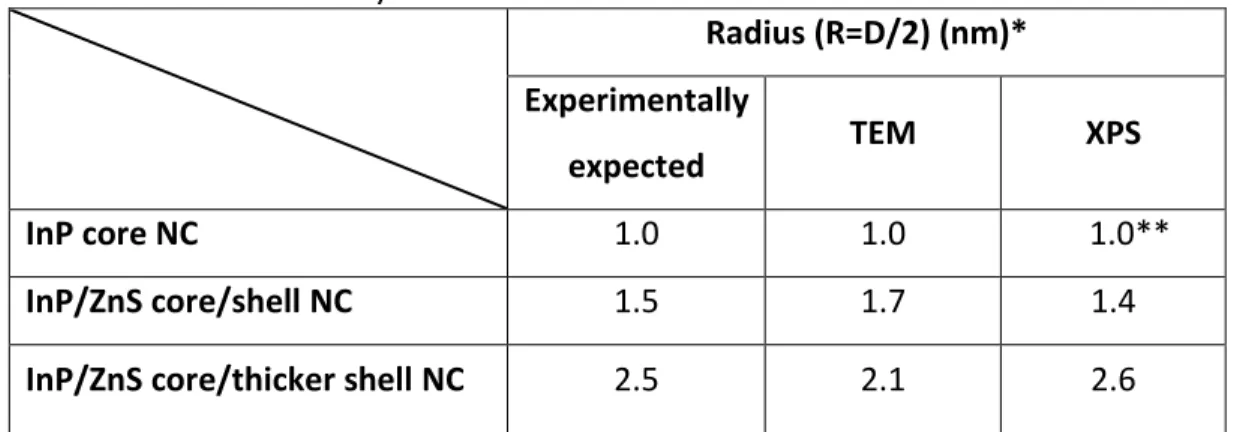
Table 3.2.2. Radii found by TEM and XPS results.
Radius (R=D/2) (nm)* Experimentally
expected TEM XPS
InP core NC 1.0 1.0 1.0**
InP/ZnS core/shell NC 1.5 1.7 1.4
InP/ZnS core/thicker shell NC 2.5 2.1 2.6
*R is the radius and D is the diameter. **InP core radius is fixed for XPS calculations.
Table 3.2.2. results are very close to the expected experimental results, which is the indication of nice coverage of ZnS shell around InP core NCs. The 2nd shell coverage is low but it is known that the resolution of XPS is higher than the resolution of TEM. Moreover, the diameters of NCs prepared are small and their crystallinity is not perfect. Therefore, it is hard to detect the correct frames for NC outer shell. The radius difference may come from these effects.
Apart from the real radius, hydrodynamic radius can also be found with the help of DLS by using software provided by Malvern. It should be noted that the found
38
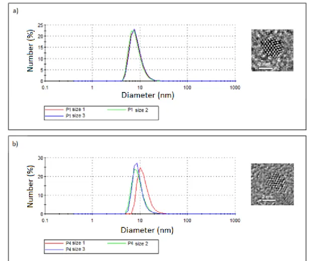
average diameters are for the case of diluted NCs with hexane because the resulting diameter is dependent on the solvent chosen. For the hexane case, hydrodynamic diameters are found as 8 nm (with a standard deviation of 5 nm) and 10 nm (with a standard deviation of 4 nm) for the InP/ZnS NCs after the 1st and 4th purifications, respectively, as shown in Figure 3.2.3. The reason of purification is to prevent additional interference of ligands and/or irrelevant particles, which may possibly adversely change the result. For the used NCs, the TEM result was 2 to 3 nm for the core/shell NCs.
Figure 3.2.3. DLS size distribution for InP/ZnS NC samples (a) after the 1st purification and (b) after the 4th purification, along with their TEM images.
39
3.3. Crystal Structure Study
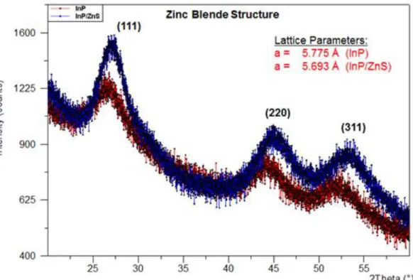
Most of the semiconductor NCs are in the crystal structure of cubic zinc blende or hexagonal wurtzite [8]. The powder X-ray diffraction pattern for InP and InP/ZnS NCs show the behaviour of zinc-blende structure as shown in Figure 3.3.1, and they have strong peaks which correspond to the (111), (220), and (311) planes.
Figure 3.3.1. XRD spectroscopy of InP core and InP/ZnS core/shell NCs with their calculated lattice parameters.
The lattice parameters shown in Figure 3.3.1 are calculated on the basis of Bragg condition. By using Bragg condition as indicated in (5) in Section 1.2.8, the interplanar distance, d, is found and then it is converted to the lattice parameter, a, for the zinc blende structure as
(15)
40
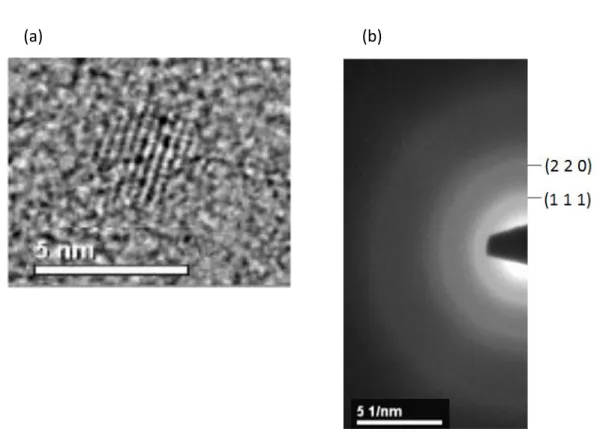
In order to define the crystal structure, similar calculations can also be carried out by using TEM results. Figure 3.3.2 and Figure 3.3.3 can be used to calculate the lattice constants for all core and core/shell NC structures. First, it is required to determine the average diameter of NCs and it is given with a sample magnified TEM image in the given figures. From the selected area electron diffraction (SAED) patterns, the interplanar distance, d for the core and core/shell NCs are found as
(16)
where RSAED (in Å) is the radius of the selected area diffraction patterns as shown in Figures 3.3.2(b) and 3.3.3(b).
(a) (b)
Figure 3.3.2. (a) TEM image (2 nm) and (b) selected area electron diffraction pattern of InP core NCs.
41
(a) (b)
Figure 3.3.3. (a) TEM image (3 nm) and (b) selected area electron diffraction pattern of InP/ZnS core/shell NCs.
After finding d, by using (15), the lattice constant, a, can be found. The results found by using both XRD and TEM are given in Table 3.3.1.
Table 3.3.1. Calculated lattice parameters by using TEM diffraction pattern and XRD results.
XRD TEM
d (Å) a (Å) d (Å) a (Å)
InP core NCs 3.34 5.775 3.28 5.687
InP/ZnS core/shell NCs 3.29 5.693 3.20 5.545
The bulk lattice constants for InP and ZnS are reported as 5.869 Å and 5.416 Å, respectively, in the literature [8]. NC lattice constants are expected to be between these values and as seen from Table 3.3.1, the results of XRD and TEM satisfy the expectation. From these results, it can be said that XRD gives more reliable results since it relies on an ensemble measurement whereas TEM uses only a small portion
42
of the sample for analysis. The problem with measuring only the small portion is that the defects of NCs affect the results more, making the measurement more dependent on the sample region chosen.
3.4. Core/Shell Study
InP core NCs typically have quantum yields around 10% and are not very stable in air conditions. Oxidization is a problem for such NCs; e.g., phosphorus (P) oxidization occurs and the oxidized NCs suffer the efficiency. However, the encapsulation of these core NCs with a wider band gap semiconductor material such as ZnS improves the efficiency and increases it up to 30-40%, and reduces or even eliminates the oxidization problem.
Proving successful shell formation is hard most of the time. Spectroscopic analyses like UV-Vis NIR spectroscopy and fluorescence spectroscopy give an insight with red shifted results for the shell growth but not a complete proof. After formation of the shell, a small red shift in the excitonic peak in UV-Vis NIR absorption spectrum and photoluminescence peak wavelength (shown with a red arrow) becomes observable in Figure 3.4.1. The shift in absorption is not readily detectable because of the large size distribution of InP/ZnS NCs. The reason of this phenomenon can be explained as a partial leakage of the exciton into the shell material [3]. However, these methods are not sufficient; they should be supported with additional structural studies. TEM and XPS are the promising tools enabling the detection of shell growth.
43
Figure 3.4.1. Absorption and PL spectra of the InP core and InP/ZnS core/shell NCs.
For our as-synthesized InP core and InP/ZnS core/shell, and InP/ZnS core/thicker shell NCs, the obtained results are presented in Figure 3.4.2 and Figure 3.4.3. In Figure 3.4.4, In 3d5/2 and In 3d3/2 peak counts, which have binding energies of 444 and 452 eV, respectively, decrease and Zn 2p3/2 peak counts (with binding energy of 1022 eV) increases with the increasing shell thickness because the incoming signal changes for all compounds when a thicker shell is formed. For In 3d cases, a zoomed figure which is depicted in Figure 3.4.3, is easier to observe the change.
44
Figure 3.4.2. XPS survey data for InP core, InP/ZnS core/shell and InP/ZnS thicker shell NCs.
Figure 3.4.3. XPS survey showing indium peaks for InP core, InP/ZnS core/shell and InP/ZnS thicker shell NCs.
45
Figure 3.4.4. XPS results of In, P, Zn, S peaks for NC of InP core (Core), InP/ZnS core/shell (CS1) and InP/ZnS core/thicker shell (CS2) samples.
So far, XPS results are compared with respect to the count numbers for the binding energies of In and Zn elements because the corresponding films are prepared with similar amount of NCs and for the same spin values. However, since the peak count also depends on the concentration of NCs on the film surface, Zn to In ratio will result in a better confirmation for the shell formation compared to the intensity evaluation. For the results taken from the data of additional shell formation experiments seen in Figure 3.4.4, the corresponding chart is obtained in Figure 3.4.5. Here the shell formation is obvious due to the increasing Zn:In ratio (faster than a straight line, which would be interpreted as an alloy). In our case, this implies that we have core/shell NCs.
![Table 1.1.2.1. Material parameters of selected bulk semiconductors [8].](https://thumb-eu.123doks.com/thumbv2/9libnet/5733767.115129/20.918.196.827.139.504/table-material-parameters-selected-bulk-semiconductors.webp)
![Figure 1.2.6.1. Schematic representation of (a) photoionization process and (b) Auger electrons [5]](https://thumb-eu.123doks.com/thumbv2/9libnet/5733767.115129/26.918.200.798.237.479/figure-schematic-representation-photoionization-process-b-auger-electrons.webp)
![Figure 1.2.7.1. Components of Zetasizer Nano series for DLS measurements [6]](https://thumb-eu.123doks.com/thumbv2/9libnet/5733767.115129/28.918.318.683.535.992/figure-components-zetasizer-nano-series-dls-measurements.webp)