This document is downloaded from DR-NTU, Nanyang Technological
University Library, Singapore.
Title
Manipulating Optical Properties of ZnO/Ga:ZnO Core-Shell Nanorods Via Spatially Tailoring Electronic Band Gap
Author(s) Zhao, Xin; Gao, Yuan; Wang, Yue; Demir, Hilmi Volkan;Wang, Shijie; Sun, Handong
Citation
Zhao, X., Gao, Y., Wang, Y., Demir, H. V., Wang, S., & Sun, H. (2015). Manipulating optical properties of ZnO/Ga:ZnO core-shell nanorods via spatially tailoring electronic band gap. Advanced Optical Materials, 3(8), 1066-1071.
Date 2015-03-30
URL http://hdl.handle.net/10220/40341
Rights
© 2015 Wiley-VCH Verlag GmbH & Co. KGaA,
Weinheim. This is the author created version of a work that has been peer reviewed and accepted for publication by Advanced Optical Materials, Wiley-VCH Verlag GmbH & Co. KGaA, Weinheim. It incorporates referee’s
comments but changes resulting from the publishing process, such as copyediting, structural formatting, may not be reflected in this document. The published version is available at:
1
DOI: 10.1002/adom.((please add manuscript number)) Article type: Communication
Manipulating Optical Properties of ZnO/Ga:ZnO Core-Shell Nanorods via Spatially Tailoring Electronic Band Gap
Xin Zhao, Yuan Gao, Yue Wang, Hilmi Volkan Demir, Shijie Wang, and Handong Sun*
X. Zhao, Y. Gao, Y. Wang, Prof. H. V. Demir, Prof. H. Sun
Division of Physics and Applied Physics, School of Physical and Mathematical Sciences Nanyang Technological University, 21 Nanyang Link
637371, Singapore
E-mail: [email protected] Prof. H. V. Demir
School of Electrical and Electronic Engineering, Block S2.1 50 Nanyang Avenue,
639798, Singapore Prof. H. V. Demir
Department of Electrical and Electronic Engineering, Department of Physics, UNAM-Institute of Materials Science and Nanotechnology
Bilkent University, Bilkent, Ankara 06800, Turkey
Dr. S. Wang
Institute of Materials Research and Engineering (IMRE)
A*STAR (Agency for Science, Technology and Research), 3 Research Link 117602, Singapore
Prof. H. Sun
Centre for Disruptive Photonic Technologies, School of Physical and Mathematical Sciences Nanyang Technological University, SPMS-PAP-01-28, 21 Nanyang Link
637371, Singapore
Submitted to
2
ZnO based nanostructures have attracted tremendous attention in the field of short-wavelength optoelectronics in the ultraviolet and blue including nano-lasers, blue light-emitting diodes (LED) and photodetectors.[1, 2] Besides the possibility of room-temperature excitonic lasing facilitated by the large exciton binding energy (~60 meV),[3] another promising property of ZnO nanostructures, especially nanorods (NRs) array, lies in the integration of optical gain media with high quality resonators.[4] However, the high surface-to-volume ratio, one of the most prominent characteristics of nanorods, seriously deteriorates the optical property. On one hand, the material-ambient interface tends to adsorb gas or ion species (such as 𝑂2− and 𝐶𝑂
32−), resulting in the lateral build-in potential and depletion region
near the surface.[5] Under such conditions, excitons are dissociated into electrons and holes, which respectively reside in the core and surface, reducing the possibility of radiative recombination. On the other hand, the density of defects is much higher near the surface than in the bulk-like core, resulting in the rise of visible deep-level emission (DLE). To suppress the nonradiative recombination and DLE, various schemes including dielectric and polymer coating,[6] excitons localization[7] as well as plasma immersion ion implantation (PIII)[8] have been applied to modify the surface composition.
Aside from the surface modification, deliberately incorporating dopants to manipulate the electrical property of the ZnO NRs is of great significance as well, which is a corner stone for high-performance optoelectronic devices.[9] However, there exists a trade-off between the electrical and optical properties of semiconductor nanostructures in this approach. Specifically, although dopants are eligible to modulate carrier concentration, high-level of doping would typically introduce extra structural defects in the near defect-free nanorods. [10] Being easily overlooked, doping is also capable of modulating the band alignment, which can be demonstrated by the band diagram of a homojunction.[2, 11] Through modulating the carrier
3
concentration by doping, electronic band structure tailoring can be achieved without coating lattice-mismatched material , in which the coated dielectric material (usually MgO) has a lower refractive index and inferior electronic property,[12] impairing the light extraction and electrode contact. Nevertheless, to the best of our knowledge, band engineering via doping has been rarely reported.
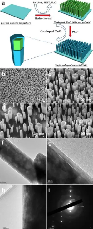
In this study, we adopted a novel strategy for growing surface doped core-shell ZnO nanorods array aiming at simultaneously enhancing the optical and electrical properties as well as improving the product yield of growth. The growth method involves two steps consisting of (i) hydrothermal growth of ZnO nanorods on p-GaN substrate as templates and (ii) subsequent coating of Ga-doped ZnO (around 2 at% of gallium) via pulsed laser deposition onto the NRs template after annealing in 3.5 Pa O2 at 700 ºC for 40 min to form
core-shell hetrostructure. The schematic illustration and details of the growth are enclosed in Figure 1a. Herein, the details of the growth and annealing are enclosed in supporting information. The key point in this strategy lies in the incorporation of gallium during the coating process, which could offer two benefits: 1) the outer shell increases the carrier concentration and conductivity without degrading the core crystal quality; 2) the n+ shell modifies the spatial band alignment and blocks the diffusion of holes from the core to the surface, which enhances optical properties by suppressing the non-radiative recombination of the holes with the trapped electrons. The resulting advantages would reveal themselves in the following photoluminescence (PL) measurements, and the underlying mechanisms are consistently studied and discussed on the basis of temperature-dependent PL and X-ray photon electron spectroscopy (XPS).
The scanning elecetron microscopy (SEM) images display the morphology changes of samples during the annealing and shell growth processes. Figure 1 (b-c) show that high-density nanorod arrays are grown perpendicular to the p-GaN substrate via the hydrothermal
Submitted to
4
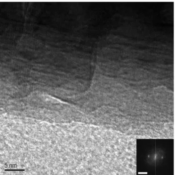
growth. The classical haxagonl morphology of ZnO reveals that NRs grow along the c-axis and are highly crystallized, providing ideal templates for the succesive shell growth. Regarding the samples shown here (synthesized using 35 mM precursor), the average diameter of NRs is around 180 nm and the aspect ratio is in the range of 5-20. In order to gurantee the credability of the following measurements and to refrain from overdue carrier depletion, nanorods with various diameters were grown by simply modulating the precursor concentration (Figure. S1). After annealing in the PLD chamber, as shown in Figure 1d, small dimples emerge at the surface of the control sample (without shell), which may be caused by the surface atoms rearrangement and accumulation of oxygen vaccancies.[13] When Ga-doped ZnO shell (around 10 nm) was coated, the density of dimples are reduced and nanorod surface become smooth (Figure 1e). Moreover, the diameter of most core-shell rods was found to be uniform from the top to the base along the axial direction, indicating the coating is free of shadow effect.[13] To better understand the crystalline quality and composition of the shells, high resolution transmission electron microscopy (HRTEM) is conducted. As shown in Figure 1 (f-h), the thickness of the doped ZnO shell is uniform along the nanorods and the boundary between the core and the shell is clearly resolved. For the straightforwardness of unambiguous observation, here we studied the sample with the thickest shell (which experienced 200 laser pulses) and the thickness was measured to be 16 nm, fairly close to the calculated 20 nm value via pre-calibration. In the selected area electron diffraction (SAED) image, there is only one single set of spots in the reciprocal space, further confirming that the NR grows along the c-axis and the shell grows epitaxially on the core.[14] Lattice fringe of the shell is shown in Figure. S2.
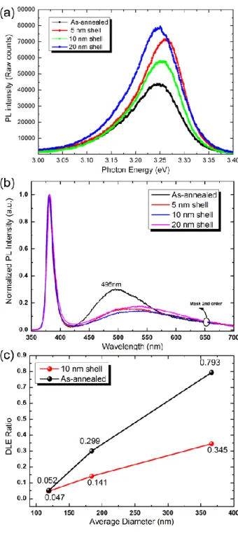
After the core-shell hetrostructure is formed, the optical property of the NRs is enhanced, especially the near-band-edge emission (around 380 nm at room temperature), which is shown in Figure 2a. The spectra of the core-shell samples did not show systematically shift in peak
5
energy, indicating this new scheme is able to improve the luminescence without drastically deteriorating the intrinsic emission. The intensity of the 20 nm thick shell sample experiences 2-fold enhancement and it is clear that the enhancement is not proportional to the shell thickness; ruling out the possibility that enhancement is simply caused by the increasing effective luminescence volume. It should be mentioned that all the samples in the optical property comparison are grown and processed in the same batch, which guarantees that the samples are comparable with each other. Figure 2b displays the normalized room-temperature PL covering the luminescence region of ZnO (350-700 nm) and unravels that that not only the near band-edge emission (NBE), but also the NBE/DLE ratio is increased by at least one fold for the core-shell samples, which indicates less localization and recombination of excitons at the defect sites (such as oxygen vacancies and Zn interstitials). Through careful comparison of the DLE spectra shape, it is found that luminescence peak position has shifted to lower energy for the core-shell sample, implying the existence of n+ shell modulates the recombination probability at different defect centers. The underlying mechanism of the NBE enhancement and modulation of DLE will be elucidated and discussed in association with the following temperature-dependent photoluminescence (TDPL) and XPS data.
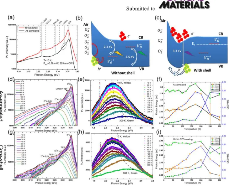
TDPL is measured using a 325 nm continuous-wave laser as the excitation source and results are presented in Figure 3. Figure 3a highlights 10 K spectra of the core-shell nanorods and as-annealed nanorods, in which the spectra are shifted in intensity for clear comparison. The NBE regions of both spectra are dominated by a broad, asymmetric peak. Regarding the as-annealed nanorods (control sample), the highest peak at 3.356 eV is assigned to the exciton bound to neutral donor, accompanied by longitudinal optical replicas at 3.290 and 3.217 eV.[15] This designation of D0X is further confirmed via fitting the peak position data with the empirical Varshini equation (Figure. S3), which quantitatively describes the dependence of peak position on temperature.[16] Moreover, the existence of high-order phonon replica
Submitted to
6
implies that crystal quality is improved during the annealing process. The obvious shoulder at 3.331 eV (Y-line) appears due to the localization of excitons at the structural defects, usually referring to defects near interface or crystal boundaries.[17] In the case of nanorods, which are primarily assumed to be single crystal in nature, the peak around 3.331 eV may be further verified as an indicator of the exciton bound to surface defects. We now turn our attention to the spectrum of NRs with gallium doped shell, where it behaved differently in two aspects. Firstly, the shoulder at 3.33 eV is largely suppressed (noticing the log scale of intensity), implying that the excitons detach from the surface structural defects. Secondly, two small peaks at 3.312 and 3.236 eV emerge at the higher energy side of D0X phonon replicas, which can be assigned to the two-electron-satellite (TES) of the incorporated gallium on the basis of peak position as well as the calculated ionization energy.[15] According to the effective mass theory (EMT), the ionization energy of the donor can be calculated from the following Equation 1.
𝐸𝐷 = 𝐸1𝑠→2𝑝+
1
4𝐸𝐷,𝐸𝑀𝑇
Herein, 𝐸𝐷,𝐸𝑀𝑇 refers to the theoretical EMT donor Rydberg energy (56 meV for gallium) and the 𝐸1𝑠→2𝑝 represents the energy spacing between 𝐷0𝑋 and TES line, which is measured
to be 42 meV in the spectrum. The donor binding energy is calculated to be 56 meV, which matches well with the measured value of gallium dopant, confirming the existence of the gallium dopant.[18]
The DLE region of TDPL spectra of both the as-anneal and core-shell nanorods from 10-300 K are shown in Figure 3e and 3h. Unlike the red-shift of the NBE, the dominating peaks of the two DLE spectra shift from 2.1 eV (10 K) to 2.45 eV (300 K) with the increasing temperature, which cannot be explained by the band gap shrinkage. If we take a closer look at the wide DLE peak, it is obvious the blue shift of the peaks results from a wane and wax
7
relationship of the two luminescence centers, namely the yellow center around 2.1 eV, corresponding to the transition from the conduction band to 𝑉𝑂++ defect center, and the green
center around 2.5 eV, correlated to recombination of electrons from 𝑉𝑂+ to the valence
band.[19] So it is intuitive to decompose the wide peak into two Gaussian peaks and Figure 3f and 3i show the fitted peak position and relative peak intensity of the constitutional peaks, respectively. The fitted peak position is in good agreement with the reported value and the adjusted R-square which indicates the quality of fitting is all above 99.9%.
Herein, as shown in Figure. 3b and 3c, we propose a novel spatial band diagram model aiming to explain the NBE enhancement as well as the changing trend of DLE components for the core-shell nanorods. Now, let us turn back to Figure. 3f and 3i. At the low temperature range (10-170 K), green and yellow components of both control and core-shell samples experience an increment in intensity, which is caused by the increased probability of excitons captured at the defects. When temperature reaches 200 K, Yellow component wanes while the green component waxes. Here, the build-up of surface potential caused by the increased concentration of thermally ionized electrons played a key role. It has been demonstrated by Simpkins et al.[20] that the energy barrier height would increase with elevated electron concentration. As a result, the built-in potential would deprive one hole from the 𝑉𝑂++defect
center and turn them into 𝑉𝑂+, leading to the competition in luminescence intensity of the two
components.
In addition, it is clear that the orange component of the core-shell NRs starts decreasing at a higher temperature than the as-annealed ones, which implies the existence of potential barrier introduced by carrier concentration difference between the core and the shell would block holes from diffusing to the surface. At a temperature higher than 250 K, intrinsic and more extrinsic carriers activated by thermal energy would elevate the Fermi level and quench the 𝑉𝑂+ defect center, which is responsible for the intensity dropping of the green component. In
Submitted to
8
this regard, the Fermi level should be close to the 𝑉𝑂+ level in the core at 300 K. In other
words, EF is 0.8 eV higher than the middle of the energy band gap, which coincides with
slightly n-type nature of the undoped core.[21] Also, we should note that the green component of the core-shell NRs is quenched at a lower temperature than the as-annealed sample. This phenomenon can be explained by the fact that electron in the n+ shell would diffuse towards the core and the EF would be higher and closer to 𝑉𝑂+ than the as-annealed sample.
It should be further emphasized that the dip in the band introduced by surface doping is also responsible for the enhancement of the NBE. It has been demonstrated that the built-in potential induced by surface adsorption would provide a powerful but unwanted non radiative recombination channel, as shown by the red arrow in the Figure 3b.[22] The energy dip introduced by our novel design partially blocks the hole from diffusing to the surface and suppresses the non radiative recombination, meanwhile it enhances the NBE.
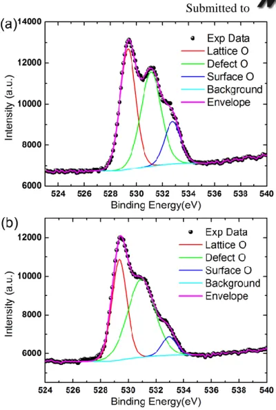
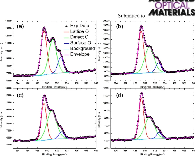
Moreover, our model is further supported by the XPS measurements. It is demonstrated by Park et al. that the oxygen peak of ZnO NRs can be decomposed into three components with different binding energy, namely, lattice oxygen OI (approximately 529 eV), oxygen around
defects OII (approximately 531 eV) and surface adsorbed oxygen OIII (around 533 eV).[23]
Regarding the core-shell NRs, the adsorbed oxygen is reduced by 50% compared to the control sample as displayed in Figure. 4a-b and Figure. S5. This phenomenon could be well explained considering that the energy dip retains both hole and electron away from surface and reducing the probability of the chemical adsorption(𝑂2−) formation.
In summary, we have proposed and demonstrated a generic strategy of surface-doped core-shell nanorods grown via simple two-step method for effectively enhancing optical and electronic properties of ZnO-based nanorods. The hydrothermal process guarantees a high product yield and successive PLD coating is also mature and scalable, which makes this methodology viable for other semiconductor nanostructures. By correlating the conjugating
9
factors like carrier concentration, optical property and surface depletion, this study provides a significant physical insight for designing high-performance optoelectronic nano devices.
Experimental Section
Core-shell ZnO Nanorods growth: Growth of the surfaced doped core-shell ZnO nanorods
array involves two steps. First, undoped ZnO nanorods are grown epitaxially on a p-GaN substrate via hydrothermal method. The precursors, namely Zn(CH3COO)2 and
hexamethylenetetramine (HMT), are dissolved in DI water to form solutions with controlled concentration, namely 25 mM, 35 mM and 50 mM, facilitating nanorods with different aspect ratios. The solution is heated in constant-temperature oven, which is kept at 95 ºC, for 150 min. Second, doped shell is coated around the NRs templates obtained in the first step. The sample is annealed under conditions of 3.5 Pa, 50 SCCM (standard cubic centimeter per minute) O2 flow for 40min to improve the crystal quality and activate surface for coating.
Successively, a thin film of Ga-doped ZnO is deposited onto the NRs template at 800 ºC via pulsed laser ablation (248 nm KrF laser, 300 mJ, 20 ns) in the same oxygen atmosphere as in the annealing process. The sample is then first cooled down to 500 ºC with a rate of 10 ºC/min descending rate, followed by natural cooling to the room temperature.
Supporting Information
Supporting Information is available from the Wiley Online Library or from the author. Acknowledgements
((Acknowledgements, general annotations, funding. Other references to the title/authors can also appear here, such as “Author-One and Author-Two contributed equally to this work.”))
Received: ((will be filled in by the editorial staff)) Revised: ((will be filled in by the editorial staff)) Published online: ((will be filled in by the editorial staff))
Submitted to
10
[1] a) D. Vanmaekelbergh, L. K. van Vugt, Nanoscale 2011, 3, 2783; b) H. Zhu, C.-X. Shan, B. Yao, B.-H. Li, J.-Y. Zhang, Z.-Z. Zhang, D.-X. Zhao, D.-Z. Shen, X.-W. Fan, Y.-M. Lu, Z.-K. Tang, Adv. Mater. 2009, 21, 1613; c) D. Gedamu, I. Paulowicz, S. Kaps, O. Lupan, S. Wille, G. Haidarschin, Y. K. Mishra, R. Adelung, Adv. Mater. 2014, 26, 1541; d) J. Song, S. A. Kulinich, J. Li, Y. Liu, H. Zeng, Angew. Chem. In. Ed. 2015, 54, 462-466.
[2] M.-T. Chen, M.-P. Lu, Y.-J. Wu, J. Song, C.-Y. Lee, M.-Y. Lu, Y.-C. Chang, L.-J. Chou, Z. L. Wang, L.-J. Chen, Nano Lett. 2010, 10, 4387.
[3] R. Chen, B. Ling, X. W. Sun, H. D. Sun, Adv. Mater. 2011, 23, 2199.
[4] A. Tsukazaki, A. Ohtomo, T. Onuma, M. Ohtani, T. Makino, M. Sumiya, K. Ohtani, S. F. Chichibu, S. Fuke, Y. Segawa, H. Ohno, H. Koinuma, M. Kawasaki, Nat. Mater. 2005, 4, 42.
[5] H. Jun-Seok, D. Fabrice, P. Julien, T. Robin, F. Pierre, D. Le Si, Nanotechnology 2011,
22, 475704.
[6] a) J. P. Richters, T. Voss, D. S. Kim, R. Scholz, M. Zacharias, Nanotechnology 2008,
19, 305202; b) K. W. Liu, R. Chen, G. Z. Xing, T. Wu, H. D. Sun, Appl. Phys. Lett. 2010, 96.
[7] R. Chen, Q. L. Ye, T. He, V. D. Ta, Y. Ying, Y. Y. Tay, T. Wu, H. Sun, Nano Lett. 2013, 13, 734.
[8] Y. Yang, B. K. Tay, X. W. Sun, J. Y. Sze, Z. J. Han, J. X. Wang, X. H. Zhang, Y. B. Li, S. Zhang, Appl. Phys. Lett. 2007, 91, 071921.
[9] V. Avrutin, D. J. Silversmith, H. Morkoc, P. IEEE. 2010, 98, 1269.
[10] H. Ding, N. Pan, C. Ma, Y. Wu, J. Li, H. Cai, K. Zhang, G. Zhang, W. Ren, J. Li, Y. Luo, X. Wang, J. G. Hou, Adv. Mater. 2014, 26, 3035.
[11] S. Chu, J. H. Lim, L. J. Mandalapu, Z. Yang, L. Li, J. L. Liu, Appl. Phys. Lett. 2008,
11
[12] S. Heitsch, G. Zimmermann, D. Fritsch, C. Sturm, R. Schmidt-Grund, C. Schulz, H. Hochmuth, D. Spemann, G. Benndorf, B. Rheinländer, T. Nobis, M. Lorenz, M. Grundmann,
J. Appl. Phys. 2007, 101, 083521.
[13] W. Liu, Y. Liang, H. Xu, L. Wang, X. Zhang, Y. Liu, S. Hark, J. Phys. Chem. C 2010,
114, 16148.
[14] X. Han, G. Wang, L. Zhou, J. G. Hou, Chem. Commun. 2006, 2, 212.
[15] B. K. Meyer, H. Alves, D. M. Hofmann, W. Kriegseis, D. Forster, F. Bertram, J. Christen, A. Hoffmann, M. Straßburg, M. Dworzak, U. Haboeck, A. V. Rodina, Phys. Status.
Solidi. B 2004, 241, 231.
[16] C. Bekeny, T. Voss, B. Hilker, J. Gutowski, R. Hauschild, H. Kalt, B. Postels, A. Bakin, A. Waag, J Appl Phys 2007, 102.044908
[17] M. R. Wagner, G. Callsen, J. S. Reparaz, J. H. Schulze, R. Kirste, M. Cobet, I. A. Ostapenko, S. Rodt, C. Nenstiel, M. Kaiser, A. Hoffmann, A. V. Rodina, M. R. Phillips, S. Lautenschläger, S. Eisermann, B. K. Meyer, Phys. Rev. B 2011, 84, 035313
[18] X. H. Wang, S. J. Xu, Appl. Phys. Lett. 2013, 102, 181909.
[19] a) H. Zeng, G. Duan, Y. Li, S. Yang, X. Xu, W. Cai, Adv. Funct Mater. 2010, 20, 561. b) Z.-M. Liao, H.-Z. Zhang, Y.-B. Zhou, J. Xu, J.-M. Zhang, D.-P. Yu, Phys. Lett. A 2008,
372, 4505.
[20] B. S. Simpkins, M. A. Mastro, C. R. Eddy, P. E. Pehrsson, J. Appl. Phys. 2008, 103, 104313.
[21] S. M. Sze, K. K. Ng, Physics of semiconductor devices, John Wiley & Sons, 2006. [22] A. van Dijken, E. A. Meulenkamp, D. Vanmaekelbergh, A. Meijerink, The Journal of
Phys. Chem. B. 2000, 104, 1715.
[23] G. C. Park, S. M. Hwang, J. H. Choi, Y. H. Kwon, H. K. Cho, S.-W. Kim, J. H. Lim, J. Joo, Phys. Status. Solidi. A 2013, 210, 1552.
Submitted to
12
Figure 1. Growth methodology and morphology evolution at different stages of the growth. a) Schematic of the two-step growth of core-shell nanorods. b) SEM image of the
hydrothermally grown undoped ZnO nanorods and central region enlarged in (c). d) SEM image of the as-annealed samples and then coated with approximately 10nm thick Ga-doped ZnO, displayed in (e). f) TEM images of a nanorod and the boundary between the core and
13
the shell is displayed in (g). i) SAED image of the central region of the resulting core-shell nanorod (h).
Figure 2. Optical properties of the core-shell and control samples. a) NBE region of PL and b) normalized PL of core-shell samples with different shell thicknesses along with the that of the control. c) DLE/NBE ratio of core-shell samples with various core diameters in comparison of the control group
Submitted to
14
Figure 3 a) 10 K PL spectra of the core-shell and control samples. Energy band diagram of b) the control and c) the core-shell samples. Temperature dependant NBE and DLE spectra of the control (d,g) and core-shell NRs (e,h) array. Constiutional components of (e) and (h) are decomposed into two components and their intensity and peak position are given in (f) and (i), in which blue curves denote the component intensity.
15
Figure 4. Element O 1s XPS spectra of a) the control sample and b) the core-shell nanorods with 10 nm thick shell.
Submitted to
16
Copyright WILEY-VCH Verlag GmbH & Co. KGaA, 69469 Weinheim, Germany, 2012.
Supporting Information
for Adv. Opt. Mater., DOI: 10.1002/adom.((please add manuscript number))
Manipulating Optical Properties of ZnO/Ga:ZnO Core-Shell Nanorods via Spatially Tailoring Electronic Band Gap
Xin Zhao, Yuan Gao, Yue Wang, Hilmi Volkan Demir, Shijie Wang, and Handong Sun*
Growth protocol:
Growth of surfaced doped core-shell ZnO nanorods arrays (NRAs) involves two-step. Firstly, undoped ZnO nanorods are synthesized epitaxially on p-GaN substrate via hydrothermal method. The precursors, namely Zn(CH3COO)2 and Hexamethylenetetramine
(HMT), are dissolved in deionized water to form solution with various concentration, namely 25mM, 35mM and 50mM, facilitating nanorods with different aspect ratio. The solution is heated at 95 ºC for 150 minutes. Secondly, doped shell is coated onto the NRAs templates gained in first step. Target we utilized here is sintered ceramic composed of 95% of ZnO (5N) and 5 % of Ga2O3. The sample is annealed in 3.5 Pa, 50 SCCM (standard cubic centimeter per
minute at STM) O2 flow for 40mins to improve the crystal quality and activate surface for
epitaxial growth. Successively, a thin film of Ga doped ZnO is deposited onto the NRs template at 800 ºC via pulsed laser ablation (248nm KrF laser, 300mJ, 25ns) in the same oxygen atmosphere as in annealing process. The sample is then firstly cooled down to 500 degree with 10 degree /min descending rate, followed by natural cooling to room temperature.
17
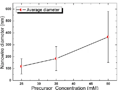
Figure S1. Average diameter of the undoped ZnO nanorods vs. the precursor concentration. The error bar denotes the standard deviation from the center value. Over 150 randomly picked nanorods are counted to generate each data point displayed in this figure to guarantee the measurement is statistically significant.
Submitted to
18
Figure S2. Lattice fringes at the surface of the core-shell nanorods sample. The shell thickness is pre-calibrated to be 20 nm (scale bar here is 5 nm). And clearly shown here, the shell is highly crystallized as amorphous. The inset is the fast-Fourier-transfer of the image and d-spacing is measured to 0.271 nm, corresponding to the (002) planes of ZnO. (The bar in the inset denotes 5 1/nm).
19
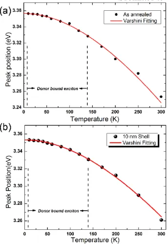
Figure S3. Varshini fitting of the dominant peak position from 10 to 140 K and the curve is extended to 300 K, which shows that the nature of dominating peak is the donor-bound exciton in the low temperature range. Considering the obvious thermal broadening effect, it is difficult to define the optical transition process from 200 K onwards.
Submitted to
20
Figure S4. O 1s XPS component comparison of a) the as-annealed and the core-shell samples with the shell thickness of b) 5 nm, c) 10 nm and d) 20 nm.
21
Figure S5, Normalized O 1s components plot of the lattice oxygen, defect oxygen and surface oxygen. With the increasing shell thickness, the surface adsorbed oxygen decreases by 50%.