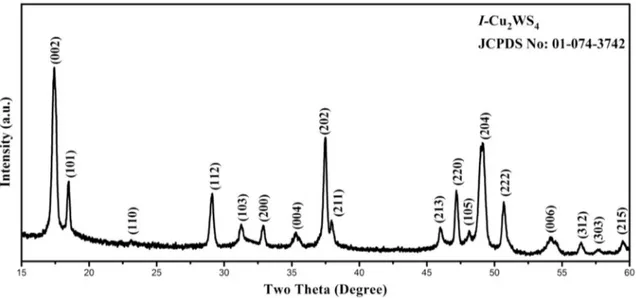
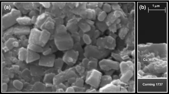
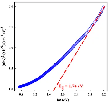
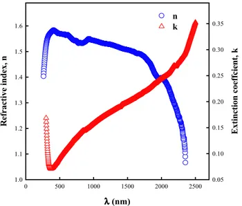
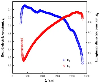
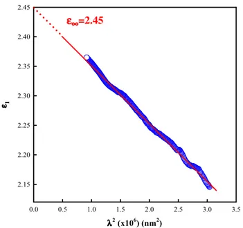
Investigation of structural, optical and dielectrical properties of Cu2WS4 thin film
Tam metin
Şekil
Benzer Belgeler
Falih R ıfkı Bey, Atatürk devrinde — mutadı veçhile — öteki arkadaşları gibi M illet Meclisine girmiş, fakat hizme tini daha ziyade kalemiyle sürdürerek
Edir.ne Rüştiye ve Öğretmen Okulu'nu bitirdi.. Taha
However, there are few studies that focus on how, in dealing with these challenges, users try to develop a sense of their audience by categorizing their Facebook friends and
Deneysel olarak test edilmiş bazı canlı aşılar koruyucu hastalıklara karşı koruyucu bağışıklık oluşturdukları bir çok araştırmacı tarafından bildirilmiştir
mathematics using the GeoGebra software on 12th grade G&T students' conceptual understanding of limits and continuity concepts. A secondary purpose was to investigate the
Benign mesothelial tumors of the urinary bladder: Review of literature and a report of a case of leiomyoma. Knoll LD, Segura JW,
Batılı bir müzik, dans ve eğlence türü olan tango, İstanbul’un eğlence mekânlarında görülmeye başlamadan çok önce, Batı müziği Osmanlı’da
Majority of student mobility and study abroad research focus on Western contexts such as the United States and the United Kingdom. This paper makes a unique
