AB-INITIO STUDY OF IRIDIUM ON
SILICON (001) SURFACE
a thesis
submitted to the department of physics
and the graduate school of engineering and science
of bilkent university
in partial fulfillment of the requirements
for the degree of
master of science
By
˙Ismail Can O˘guz
August, 2013
ABSTRACT
AB-INITIO STUDY OF IRIDIUM ON SILICON (001)
SURFACE
˙Ismail Can O˘guz M.S. in Physics
Supervisor: Prof. Dr. O˘guz G¨ulseren August, 2013
Self-assembled nanowire growth on semiconductor surface is based on deposing sub-monolayer material over the surface. Even though high resolution STM im-age gives plausible surface analysis, determination of the nanowire structure is the most di↵ucult part of these experiments. Due to the this reason, first-principles investigation is essential to understand the one dimensional nanowire structure grown over the surface as well as the STM images of these structures. Recently, iridium silicide nanowire on Si (001) surface is observed. In this thesis, we study formation of the nanowire after deposition of Ir on Si(001). Ab-initio plane wave pseudopotential calculations are performed for number of iridium silicide nanowires generated by increasing iridium coverage on Si(001) surface. For the iridium coverage as 0.125 ML, the possible nanowire formation is analyzed and its calculated STM images are compared with experimental STM image. As a result of our detailed analysis, we suggest that the STM image observed at experiment doesn’t consist of Ir atoms since Ir atom tends to be buried into the Si bulk. We model the possible nanowire formation which is consistent with pseudo-STM calculation. According to our model, iridium is placed at the troughs between the dimer rows on the surface and it creates a structure by breaking the Si dimer bonds. The coverage implied by the model, is consistent with experimental num-bers.
¨
OZET
S˙IL˙ISYUM (001) Y ¨
UZEYLER˙INDE ˙IR˙IDYUM
ATOMLARININ ˙ILK PRENS˙IP HESAPLARDAN
˙INCELENMES˙I
˙Ismail Can O˘guz Fizik, Y¨uksek Lisans
Tez Y¨oneticisi: Prof. Dr. O˘guz G¨ulseren A˘gustos, 2013
Y¨uzeyde katman-altı miktarda malzemeyi biriktirerek kendili˘ginden y¨uzeyde nan-otel b¨uy¨ut¨ulebilir. Y¨uksek ¸c¨oz¨un¨url¨u taramalı t¨unelleme mikroskobu y¨uzey hakkında detaylı bilgi vermesine ra˘gmen, bu deneylerin en zor kısmı, nanotelin yapısının belirlenmesindedir. Bu sebepten dolayı, y¨uzeyin nasıl g¨or¨und¨u˘g¨un¨u ve bir boyutlu yapıların y¨uzeyde nasıl b¨uy¨ud¨u˘g¨un¨u anlamak i¸cin yo˘gunluk fonksiy-onel teorisi analizi yapılmasının b¨uy¨uk faydaları vardır. Nuri Oncel ve ek-ibi silisyum (001) y¨uzeyi ¨uzerinde iridyum silisli bile¸simden olu¸san nanoteller g¨ozlemledi. Bu tezde, iridyumun silisyum (001) y¨uzeyi ¨uzerinde biriktirilmesin-den sonra olu¸san nanotellerin yapısı ¸calı¸sıldı. T¨um hesaplamalar ilk prensip yo˘gunluk fonksiyonu teorisi kullanıldı ve farklı yapıda iridyum silisli bile¸simden olu¸san nanotel yapıları iridyum atomlarının silisyum (001) y¨uzeyindeki kap-sama alanını artırarak olu¸sturuldu. ˙Iridyumun kapsama alanı miktarı 0.125 ML(tek katman) se¸cildi˘ginde olu¸san nanotellerin geometrik yapısı incelendi ve hesaplanan taramalı t¨unelleme mikroskop g¨or¨unt¨uleri deneysel g¨or¨unt¨ulerle kıyaslandı. Bu hesaplamalar sonucunda, iridyum atomu silisyum kristalin i¸cine girmeye ¸calı¸sıyor sonucuna ula¸sıldı˘gından dolayı, deneyde elde edilen taramalı t¨unelleme mikroskop g¨or¨unt¨ulerindeki yapıların ˙Iridyum atomundan kaynaklan-madı˘gı sonucuna varıldı. Yapılan t¨um hesaplar incelendi˘ginde, iridyum, silisyum dimer atomlarının arasındaki bo¸slu˘ga yerle¸since olu¸san geometrik yapı bize en d¨u¸s¨uk enerjili silisyum (001) y¨uzeyi yapısını verdi˘gi bulundu. Bu yapının taramalı t¨unelleme mikroskop g¨or¨unt¨uleri hesaplandı˘gında, deneysel STM g¨or¨unt¨uleriyle tutarlı bir g¨or¨un¨um sa˘glamaktadır.
Anahtar s¨ozc¨ukler : ˙Iridyum-silisli bile¸simden olu¸san nanotel, Silisyum (001) y¨uzeyi, Ba˘glanma enerjisi, Hesaplanmı¸s STM g¨or¨unt¨us¨u, Yo˘gunluk fonksiyonel teori.
Acknowledgement
I would like to firstly acknowledge the amazing support, wisdom, and guidance from my supervisor Prof. O˘guz G¨ulseren. He always gives me constructive com-ments and warm encouragement. His guidance helped me in all the time of research and writing of this thesis.
Besides my advisor, I would like to thank the rest of my thesis committee: Assoc. Prof. Dr. Hande To↵oli and Assoc. Prof. Dr. Ceyhun Bulutay for their encouragement, insightful comments.
I have greatly benefited from Ozan Yerli and Kutan G¨urel. Without their guidance and persistent help, this thesis would not have been possible.
I would like to o↵er my special thanks to H¨useyin S¸ener S¸en, Yaprak Korkmaz and Benjamin Reimold.
Last but not the least, I would like to thank my family: my parents Sevim O˘guz and Mehmet O˘guz, for giving birth to me at the first place and supporting me spiritually throughout my life.
The numerical calculations reported in this thesis were performed at TUBITAK ULAKBIM, High Performance and Grid Computing Center (TRUBA Resources)
Contents
1 Introduction 1
1.1 Epitaxial Growth of Nanowires on Surfaces . . . 2
1.2 Experimental Characterization . . . 2
1.3 Iridium Silicide on Silicon (001) surface . . . 3
1.4 Density functional theory study of nanowire formation . . . 5
1.5 Iridium . . . 6
1.6 Outline of the Thesis . . . 7
2 Computational Methods 8 2.1 Introduction . . . 8
2.1.1 The Born-Oppenheimer approximation . . . 9
2.1.2 Hartree and Hartree Fock Methods . . . 10
2.2 Density Functional Theory . . . 13
2.2.1 Hohenberg-Kohn Theorem . . . 13
CONTENTS vii
2.2.3 LDA(Localized density approximation) . . . 15
2.2.4 GGA(Generalized Gradient approximation) . . . 16
2.2.5 Periodic Boundary Conditions . . . 16
2.2.6 Bloch Theorem . . . 18
2.2.7 Sampling Brillouin zone . . . 18
2.2.8 Plane wave basis set . . . 19
2.2.9 Pseudopotential . . . 19
2.2.10 Hellmann Feynman Theory . . . 20
2.3 Surfaces . . . 21 2.4 Supercell Method . . . 21 3 Computational Details 23 4 First-principles investigation 25 4.1 Silicon (001) surface . . . 25 4.1.1 Dimer reconstruction . . . 28
4.1.2 Surface and bulk states of Si (001) . . . 29
4.1.3 2+1 Dimer Vacancy on Si (001) surface . . . 32
4.2 Iridium coverage on Si (001) surface . . . 33
4.2.1 0.125 ML coverage deposition over Si (001) surface . . . . 33
CONTENTS viii
4.2.4 DFT study of Ir Silicide Nanowire . . . 47
4.2.5 Suggested nanowire model . . . 49
4.2.6 Ir-Si Nanowire model . . . 51
4.2.7 Buried iridium on Si (001) surface . . . 55
5 Conclusion 56
List of Figures
1.1 STM image of the Ir silicide nanowires . . . 4
1.2 STM line scan across and along dimer . . . 4
1.3 Tentative Model of Iridium Silicide Nanowire . . . 5
2.1 Coulomb potential and pseudo wavefunction of valence electron in the core region . . . 20
2.2 Schematic illustration of supercell geometry for a surface of a bulk solid . . . 22
4.1 Si slab structure representing (001) surface . . . 27
4.2 Side view of silicon (001) (2x4) surface unitcell . . . 28
4.3 Top view of silicon (001) (2x4) surface unitcell . . . 28
4.4 Schematic representation of surface Brillouin Zone for Si (001) p(2x1) surface unitcell . . . 30
4.5 Surface and bulk states of Silicon (001) surface . . . 31 4.6 Schematic representation of 2+1 dimer vacancy and relaxed geometry 32
LIST OF FIGURES x
4.8 Single iridium atom adsorbtion on p(2x4) Si(001) surface . . . 35 4.9 Schematic representation of position of adsorbed Ir dimer on
p(2x4) Si (001) surface . . . 37 4.10 Adsorbed Ir dimer on p(2x4) Si(001) . . . 37 4.11 Adsorbed Ir dimer on p(2x4) Si(001) surface . . . 38 4.12 Schematic represantation of Ir adsorption on c(2x4) Si (001) surface 40 4.13 Relaxed geometric image of substituted Ir atom over c(2x4) Si(001) 40 4.14 Relaxed geometric image of substituted Ir atom over c(2x4) Si(001) 41 4.15 Side view of Ir nanowire growth on p(4x2) Si(001) surface . . . 42 4.16 Top view of Ir nanowire growth on p(4x2) Si(001) surface . . . 42 4.17 Adsorbed Ir atoms at terrace Si (001) surface . . . 44 4.18 Side view of adsorbed 1-2-3-5-6 Ir atoms on p(2x4) Si(001) surface 45 4.19 Top view of adsorbed 1-2-3-5-6 Ir atoms on p(2x4) Si(001) surface 45 4.20 Side view and top view of adsorbed 8 and 10 Ir atoms on p(2x4)
Si(001) surface . . . 46 4.21 Unrelaxed 6 Ir atom per (4x2) unit cell and relaxed geometric
Ir-silicide nanowire . . . 47 4.22 Unrelaxed 8 Ir atom per (4x2) unit cell and relaxed geometric
Ir-silicide nanowire . . . 48 4.23 Unrelaxed 10 Ir atom per (4x2) unit cell and relaxed geometric
Ir-silicide nanowire . . . 48 4.24 Unrelaxed 12 Ir atom per (4x2) unit cell and relaxed geometric
LIST OF FIGURES xi
4.25 Suggested nanowire model p(2x4) . . . 49
4.26 Charge density contour of suggested nanowire model . . . 50
4.27 Suggested nanowire model p(4x2) . . . 50
4.28 Three dimensional STM image of Oncel et al. model . . . 51
4.29 Ir-Si nanowire model . . . 51
4.30 Ir-Si nanowire model . . . 52
4.31 Band diagram of iridium adsorped Si (001) surface . . . 52
4.32 Buried iridium on p(2x2) Si (001) surface . . . 53
4.33 2 dimensional STM image with respect to Bias Voltage, distance of surface . . . 54
4.34 Buried iridium on Si (001) surface . . . 55
List of Tables
4.1 Relaxation of the slab structure with di↵erent number of layers . . 26
4.2 Total energy of reconstructed silicon (001) surface . . . 29
4.3 Single Ir atom adsorption on p(2x4) Si (001) surface . . . 36
4.4 Adsorbed Ir Dimer on p(2x4) Si (001) surface . . . 39
4.5 Substituted Ir atom and their substitution energy . . . 41
4.6 Ir Nanowire growth mechanism on p(4x2) Si(001) surface . . . 43
4.7 Ir Nanowire growth mechanism at terrace Si(001) surface . . . 44
4.8 Iridium nanowire growth on p(2x4) Si (001) surface . . . 47
4.9 The total energy values of stable iridium silicide nanowire . . . 49
Chapter 1
Introduction
The micro electronic industries always try to produce the most efficient and the smallest device. This analysis created a perception, which is, at lower dimen-sion there could be a circuit technology which drives us to understand the elec-tronic structure of the material and how it behaves under microscopic level. The nanowires can be good candidate to fill this analysis.
The nanowire technology adds a new dimension to the micro-electronic in-dustry. They can be used as electronic devices and biological sensors. These possible structures also show exotic physical phenomena associated with 1D sys-tem like Peirls instability [1], charge density waves(CDW) [2] and Luttinger liquid behavior [3].
Understanding of the nanowire growth mechanism is a popular research topic of applied condensed matter; and its theoretical description continue to attract interest in quantum modelling research. There are several ways of synthesizing a nanowire. One of them is called bottom-up technique. This technique is based on combination of constituent adatoms. The other is the top-down technique. For this method, lithography is used to reduce large pieces of material to small pieces.
1.1
Epitaxial Growth of Nanowires on Surfaces
Self–assembly nanowire growth on surface [4] is one example of the bottom-up technique. By using this approach, several nanowire structures are realized over semiconductor surfaces. Experimental realization is the same as deposition of adatom over the surface. Its fundamental di↵erence is the value of coverage. If the number of transmitted atom is chosen such that less than the number of surface atom, this type of coverage is called sub-monolayer coverage. The deposition rate plays vital role to estimate the amount of coverage and it is calibrated and measured with the help of Auger spectroscopy. The final step to form the nanowire is annealing process. After heating up the sample, the di↵erent kind of surface crystal structure can be observed.
1.2
Experimental Characterization
The geometric structure of composite molecule at surface can be observed by using Scanning Tunnelling Microscopy (STM) and Low Energy Electron Di↵raction (LEED). STM image gives the change in tunneling current with respect to local position of tip. It shows how the density of state is changing while the tip scans the surface; hence, it gives physical structure of molecule which is located at surface of material. LEED is also used to determine the surface structure. When the low energy electron is bombarded over the surface of material, the di↵racted electron generates the spot on fluorescent screen, thus the position and symmetry of spot gives the information of surface Bravais lattice structure. After the sample is heated up or is coated with di↵erent material, the LEED image shows how the surface structure is changing. Thus STM and LEED enable us to understand how the nanowires are composed over surface.
In recent decades, there are several experiments performed to observe nanowire by using self-assembly nanowire growth mechanism. For example, us-ing low deposition rate, O. G¨url¨u et al. partially coated Ge(001) surface with Pt adatom and self-assembled NWs are observed after annealing it at 1050K. [5]
1.3
Iridium Silicide on Silicon (001) surface
Oncel et al. [6] observed iridium silicide at silicon (001) surface and they call these structural constituent as iridium-silicide nanowire. According to their high resolution STM images, these NWs are aligned parallel [110] direction. In order to observe iridium-silicide compounds, Oncel et al. exposed various silicon wafers to LEED and deposited Ir monolayer over Si(001) surface. After that, they analyzed how the surface of silicon changes while increasing annealing temperature.
Initially, Si(001) surface is observed as p(2x1) pattern at LEED. After adding Ir mono-layer, the surface pattern became p(2x2) pattern. While increasing an-nealing temperature as 700K, 800K, 900K, and 1000K, this pattern didn’t change. But when temperature was increased to 1250K, the p(2x1) pattern appeared again. After that, annealing temperature is lowered to 700K; however, the char-acteristic p(2x1) pattern didn’t change. This permanent loss of p(2x2) pattern is attributed to di↵usion of Ir atoms into the bulk of silicon crystal and also there is an extra comment that Ir atoms can evaporate from Si surface. They again send one mono-layer Ir to surface. At this time, p(2x2) pattern is observed using LEED. According to the STM image of Ir deposited silicon surface, the Ir-Si ter-race is seen as parallel to [110] plane, which is parallel to dimer row of clean Si surface.
They also deposited 0.125 ML of Ir to study the initial stage of growth of Ir silicide terrace. After annealing at 700K, the same pattern is observed at LEED. They observed vacancy line dimer (VLD) on Si (001) surface. The same defect is also observed at Pt induced Ge(001) reconstruction.
Figure 1.1: STM image of the Ir silicide nanowires (Reproduced from reference [6])
Figure 1.2: STM line scan across and along dimer (Reproduced from reference [6])
Three dimensional STM image of Ir-Silicide NW is shown on figure 1.1. The symmetric lattice vectors are drawn over image. The brighter part of STM image is attributed to Ir atom, while the dimer part is assigned to silicon dimer. The line scan graph with respect to atomic position is shown on figure 1.2. The distance
between the taller part is 0.7nm. This amount is close to the distance between two neighboring Si dimer row. The other lattice constant which is along with the NW is 0.9nm. This distance is three times longer than the distance between Si dimer along the row. They also propose a model for Ir-Si NW. According to their model, Ir atom is replaced with Si dimer. The model picture is shown below:
Figure 1.3: Tentative Model of Iridium Silicide Nanowire (Reproduced from ref-erence [6])
1.4
Density functional theory study of nanowire
formation
Up to this point, the experimental study is explained on the NW formation over semiconductor surface; however the NW formation needs to be analyzed in terms of structure from atomic description. By using DFT based calculations, we can answer the questions such as which position at Si (001) surface is the most stable position for Ir atom, how Ir atom behaves at Si surface and whether NW formation is possible at Si surface or not. After obtaining the answer of those questions, we can compare the STM image with calculated STM image by adding sample bias voltage to the Fermi level. This analysis can reveal the detail of structure which is seen in the STM image and find out whether NWs form over the semiconductor surface.
At 2003, Gurlu et al. produced array of nanowires by deposing Pt on a Ge(001) and their geometric structure has been analyzed by using scanning tun-neling microscopy (STM) and (STS). These methods are also used to characterize
of the structure by using STM one cannot be sure about since the tunneling cur-rent of the STM is related with charge density and LDOS at Fermi level rather than chemical species directly so, they provide only tentative model which shows atomic structure of Pt nanowire.
After this observation, several studies were carried out to understand the exact nature of this formation from theoretical point view [7–12].
1.5
Iridium
Iridium is one of platinum group metal. These metals are known as noble metal since they are resistant to oxidation and corrosion. Most of metals don’t have such a property. For that reason, iridium is accepted as significant material at solid-state device fabrication. Iridium also is used as needle of STM device. The tip of STM should be composed by a rare material which is resistant to any phys-ical phenomena and it shouldn’t be oxidized; therefore the platinum metals are chosen as composite material of STM tip. The other application area of iridium is expected from iridium structure that can be formed as nanowire. The nanowire technology is developing under laboratory condition. These structures are ex-pected to be replaced with carbon nanotube and, in the near future, they will play vital role at circuit technology such as gate technology to control Schottky barrier and also they will be used as biological sensor. For that reason Ir nanowire is needed to be analyzed to understand its technological application area. Nuri Oncel et al. carried out an experiment at 2012 by deposing Ir monolayer on Si(001) surface and iridium-silicide nanowire structure is observed under high resolution STM analysis. However, STM image is based on amount of current which is read on under quantum tunneling technique and it says the how much current changes with respect to position of tip. For that reason, the STM has lack of chemical sensitivity and it can not say exactly which element is seen at image. In order to understand the growth mechanism of nanowire at surface, the system needed to be analyzed in terms of first principle investigation.
1.6
Outline of the Thesis
In this thesis, we present a computational investigation of the Ir nanowires over Si surface from first-principles calculations based on density functional theory (DFT). The most probable structures are analyzed and their simulated STM images are compared with the experimental STM image. The Si(001) surface is modeled by periodically repeated slabs of 5 layers of Si. 0.125 ML deposition is simulated by placing one Ir atom on the surface per eight Si atoms. The process of formation of NW is driven by increasing Ir adatoms over silicon. As a result of computational study, we predict the structure of Ir NWs which are observed by STM and consist of Si atoms.
The outline of this thesis is as follows: In Chapter 2, we briefly summarize the basics of DFT, and its applications are reviewed. In chapter 3, the Si (001) surface is studied, its surface reconstruction is investigated by using total energy calculations and changes in the Si surface are investigated while increasing Ir submonolayer coverage. Pseudo STM images are obtained by changing the sample bias voltage. Finally, the composed NWs are investigated by separating them from Si surface. DFT-based calculations are analyzed to estimate that whether absorbate NWs can be stable or not without sitting over Si surface.
In the last chapter, the possible Iridium silicide nanowire geometric struc-ture is discussed. The experimetal STM image is compared with the calculated STM image of stable Ir silicide structure based on plane wave pseudopotential calculations.
Chapter 2
Computational Methods
2.1
Introduction
The electronic properties of matter is predicted by using quantum mechanics and statistical mechanics. Hamiltonian of a many body system can be writen as
ˆ H = ¯h 2 2me n X i 52i m X I ¯h2 2MI 5 2 I + 1 2 n X i n X j6=i e2 |ri rj| + n X i m X I e2Z I |ri RI| + 1 2 m X I m X J6=I e2Z IZJ |RI RJ| (2.1)
SI unit system is used to write many body Hamiltonian. ~ri and ~RI describes
the position of electron and ion respectively. The first and second term repre-sent the kinetic energy of the electron and the ion. The third term is electron-electron interaction. The fourth term describes the ion-electron-electron interaction and the last term is ion-ion interaction. When this Hamiltonian is substituted into the Schr¨odinger equation, the resulting system is analytically intractable. There-fore, we have to use some approximation methods to be able to perform the calculation.
2.1.1
The Born-Oppenheimer approximation
The ion is a massive object compared to the electron, the mass of the ion is three orders of magnitude larger than the mass of th electron. Hence, when the mass of the ion and the electron are compared, it is realized that the force which are applied to the particle is same but their motion is di↵erent. This situation let us use an approximation which treats the nucleus fixed. Hence, we can seperate the total wavefunction into two distinct wavefunction. This approximation is called Bohr-Oppenheimer Approximation [13] (or Adiabatic approximation). It states that the change in the varying wavefunction of nucleus due to the Coulomb interaction is so slow when compared to its e↵ects on wavefunction of electron.
The total wave function can be written as
i(r, R) = n(R, r)✓n(R) (2.2)
Substituting this into Schr¨odinger equation results the separation of ionic and electronic coordinates, described by these two equation:
X I ¯h2 2MI 5 2 I + X I<J ZIZJe2 |RI RJ| + Eel(R) ✓(R) = "✓(R) (2.3) ¯h2 2me X i 52 i + X i<j e2 |ri rj| X i,I e2Z I |ri RI| R (r) = Eel(R) R(r) (2.4)
The first equation describes the ionic degree of freedom. The second equa-tion governs the electronic coordinates where the electrons are moving under the e↵ective potential from all of frozen ions.
2.1.2
Hartree and Hartree Fock Methods
Born-Oppenheimer approximation simplifies the Schr¨odinger equation of the many body system; however, the equation is still very difficult to solve. The main di↵uculty comes from the electron-electron interaction. In 1921, Hartree proposed a method [14, 15] to simplify the electron-electron interaction. Ac-cording to the Hartree method, the single electron is subjected to an e↵ective potential which is created by the ions and other electrons and the total electron wavefunction is written as a product of each single electron wavefunction:
(r1, r2, r3...rn) =
Y
i
(ri) (2.5)
The expectation value of Hamiltonian can be written as
< H >=X i Z ⇤ i(r)( 52 2 + Vion) i(r) dr + 1 2 X i X j6=i Z drdr0| ⇤ i(r)|2| j(r 0 )|2 |r r0 | (2.6) Atomic unit system is used to write the equation above. The second term of equation is called as Hartree energy which represent the electron-electron in-teraction. We assume that this state is a stationary state. Thus, any variation in the wavefunction will give zero variation in the energy. Using the variational calculation method and applying the constraint thath i| ii = 1 the equation can
be minimized to the Hartree single-particle equation.
i [< H > X j ✏j Z | j|2dr] = 0 (2.7) which yields ( 5 2 i 2 + V ion) i(r) + X j6=i Z d´r| j(´r)| 2 |r ´r| i(r) = ✏i i(r) (2.8)
In order to solve this equation, described in the flowchart below, initially the charge density is described in terms of single electron eigenstates and then following charge density is used to construct Hartree potential. After solving the Hartree equation, the charge density of new wave function is compared with the initial guess. If the di↵erence between charge density is larger than a tolerance, the loop goes back to second stage and a new wavefunction is substituted into the Hartree potential and the charge density. If the di↵erence is smaller than tolerance, the loop stops, thus we reach the true wave function. This method is also known as self-consistent method.
Choose in i (r) Construct ⇢in(r) =P i| ini (r)|2, Vion(r) + VHi (r, ⇢ini ) Solve [ ¯h2 2me 5 2
r+Vion(r) + ViH(r, ⇢ini )] iout(r) = ✏outi iout(r)
Construct ⇢out(r) =P i| outi (r)|2) Compare ⇢out(r) to ⇢in(r) |⇢out(r) ⇢in(r)| < tol iin(r) = outi (r) STOP Go to 2
In this approximation, the energy is written as
EH = N X i ✏n 1 2 Z Z ⇢(r)⇢(´r) |r ´r| drd´r (2.9) The factor of 1
2 appears in the second term to avoid double counting.
Hartree approximation is not sufficient to describe the fermionic nature of the electron since the many body wave function should be antisymmetric. Where-upon, Fock [16] described the many body wavefunction as antisymmetric product
of N-single electron wave function which is known as Slater determinant [17]; = p1 N ! 1(r1) 1(r2) . . 1(rn) 2(r1) 2(r2) . . 2(rn) . . . . . . . . . . . . . . . n(r1) n(r2) . . n(rn) where i(ri) = i(ri) (si) (2.10)
(s) is spin component of eigenvalue of a single particle. It can be either up or down.
The same procedure is followed to obtain the ground state energy. In contrast to the Hartree approximation, there is an extra term which is called the ”exchange term”. This term arises from the fact that electrons with the same spin should be seperated. This change reduces the Coulomb energy.
( 5 2 i 2 + V ion) i(r) + X j6=i Z dr| j(´r)| 2 |r ´r| i(r) +X j si,sj Z d´r ⇤ i(´r) j(´r) |r ´r| i(r) = ✏i i(r) (2.11)
Hartree-Fock method doesn’t give correct ground state energy since one Slater determinant is not adequate to describe fully interacting fermionic system, corre-lations of many body electronic motion are missing. The di↵erence between total energy based on DFT calculation and H-F energy is called correlation energy. It is a good method for few electron systems. But when the number of electron is increased, the computational time increases rapidly.
2.2
Density Functional Theory
In 1920 when Hartree-Fock method was discussed, Thomas and Fermi [18, 19] defined the full electron density without referring to electronic orbitals. Although this theorem doesn’t include exchange and correlation energy, it is regarded as precursor of the Density Functional Theory. DFT method was developed to overcome the problems of Hartree-Fock. For this method, the total energy is calculated by minimizing the charge density rather than the wave function. DFT describes many body systems from electronic density. With the help of Kohn-Sham equation, DFT is converted to a practical methodology.
2.2.1
Hohenberg-Kohn Theorem
Hohenberg and Kohn [20] postulated two fundamental theorems of DFT. These theorems are valid for any interacting system in an external potential. The first theorem states that the electron density determines the potential an in turn the Hamiltonian operator. With the knowledge of Hamiltonian, all properties of the system is derivable from the known Hamiltonian. Thus, the external potential is uniquely determined by the electron density.
E[⇢] = F [⇢] + Z
Vext(r)⇢(r)dr (2.12)
The second theorem states that there exists a unique functional (F [⇢]) of particle density that describes the ground state energy and it gives lowest energy if and only if input charge density is the true ground state charge density.
2.2.2
Kohn-Sham approach
F [⇢] = Ts[⇢] + 1 2 Z Z ⇢(r)⇢(´r) |r ´r| drd´r + Exc[⇢] (2.13) In this equation, there is a problem arising from kinetic energy part. At the beginning of 1920, Thomas-Fermi model was used to define kinetic energy part of many-body Hamiltonian. But it didn’t include the non-local characteric feature of electron . For this reason, Kohn-Sham [20,21] equation is developed to convert the interacting electron into equivalent non-interacting problem. Thus, the charge density can be written in terms of the single particle wavefunction.
⇢(r) = 2 X s=1 Ns X i=1 | i,s(r)|2 (2.14) T [⇢] = 2 X s=1 Ns X i=1 =h i,s| 5 2 2 | i,si (2.15)
This equation uses KS orbitals to minimize the kinetic energy by applying the constraint R ⇢(r)dr = N . In principle, these orbitals are just mathematical expression rather than a true electronic orbitals. They don’t have any physical meaning. Its eigenvalue is derivative of the total energy with respect to the occupation number of these states. Thus, e↵ective potential can be written
VKS(r) = Vext(r) + VH(r) + Vxc(r) (2.16)
where VH is called the Hartree potential
VH(r) =
Z ⇢(´r)
|r ´r|d´r (2.17)
The exchange-correlation potential can be derived by functional derivative of Exc[⇢]
Vxc=
Exc[⇢]
⇢(r) (2.18)
Thus, the many body hamiltonian is reduced to a single particle Hamiltonian which involves an e↵ective potential.
¯h2 2m 5
2+V
KS(r) i(r) = ✏i i(r) (2.19)
As described in the flow chart below, the single particle Kohn-Sham equation is solved iteratively. When the output charge density is consistent with itself, the loop is stopped and we obtain the true charge density. Using the knowledge of the charge density, we can calculate the energy of the many body system and the forces.
Choose reasonable charge density ⇢(r)in =PN i i(r) Calculate VH i (⇢in) VXC(⇢in) Solve ⇥ 2m¯h2e 52 r+Vext(r) + ViH(r) + VEX(r) ⇤ out i (r) = ✏outi iout(r) Calculate ⇢out(r) =P i| outi (r)|2) Compare ⇢out(r) to ⇢in(r) |⇢out(r) ⇢in(r)| < tol ⇢in(r) = ⇢out(r) STOP Go to 2
While calculating the total energy of the single non-interacting electron, Hartree and exchange-correlation terms are counted twice. That’s why these terms needs to be subtracted.
E[⇢] = N X i ✏i 1 2 Z 2⇢(r)⇢(´r) |r ´r| d 3rd3´r 1 4 Z µxc⇢(r)d3r + EN[R] (2.20)
2.2.3
LDA(Localized density approximation)
cal-energy needs to be approximated. Local density approximation [22] (LDA) as-sumes that Exc is an integral over all space with ✏homxc [⇢(r)] density at each point
which is the same as the homogenous electron gas with that density. Exc[⇢(r)] = Z ✏XC(r)⇢(r)dr (2.21) and ELDA XC [⇢(r)] ⇢(r) = ⇥ ✏XC[⇢(r)]⇢(r) ⇤ ⇢(r) (2.22)
LDA works good for homogenous system; however, for systems where elec-tron gas density deviates largely, LDA fails due to non-locality of Exc. LDA
results higher binding energy and underestimates the chemical bond length, the interatomic distance and the bond angle.
2.2.4
GGA(Generalized Gradient approximation)
The exchange-correalation energy is calculated within GGA [23] by evaluating integral of function of charge density depends on the density itself as well as its gradient.
ExcGGA[⇢] = Z
dr⇢(r)✏GGAxc (⇢(r);5⇢(r))) (2.23)
In general, GGA estimate binding energy more accurately than LDA. This approximate is utilized in the formulation of Perdew-Wang 91 (PW91) [24] and the Perdew-Burke-Erzenhorf(PBE) functional.
2.2.5
Periodic Boundary Conditions
As indicated at Bloch Theorem, the plane wave representation of electronic wave function should include a parameter which describes the geometric structure of
material and also it should obey the restriction arisen of periodic boundary con-ditions. In order to obtain the plane wave representation of electronic wave function, we should know how symmetric boundary conditions are implemented in the Bloch theorem to define the crystal structure. Primitive lattice vectors describes the structure of crystal by using translation vector.
R = c1a1+ c2a2+ c3a3 (2.24)
a1, a2, a3 are primitive lattice vector of real space
Crystal structure shows invariance under any translation.
n(r + T) = n(r) (2.25) As shown at 2.25, the charge concentration, electron number density and magnetic moment density is invariant under T. [25]
In order to define electronic structure of material, one has to choose a basis vector which describes the momentum space of crystal structure. The momentum space also shows periodic features which are derivable by using primitive lattice vector. It is inverse of real space and known as reciprocal space.
G = v1b1+ v2b2+ v3b3 (2.26)
b1, b2, b3 are primitive lattice vector of reciprocal space and they are
orthog-onal to two axis vector of the crystal lattice. G is reciprocal lattice vector and by using it, we can obtain this equation:
e(iGR) = 1 (2.27)
Thus we have obtained the translational symmetry under any translation. n(r + T) = n(r) =XnGexp(iG.R) (2.28)
2.2.6
Bloch Theorem
Using the above presented approximation is not enough to solve the many body particle problem since there are infinite number of non-interacting electrons mov-ing in a static potential, infinite number of nuclei remain to be solved . The main problem is that a wavefunction of each electron must be calculated and required basis set to satisfy boundary condition of crystal is infinite. In order to overcome these problems, the Bloch Theorem is used to make these calculations simpler [25] Bloch theorem states that each electronic wavefunction can be writ-ten in the form of a plane wave phase factor times a function depends periodic structure of particle. [26]
i,~k(r) = ui,~k(r)e
ikr (2.29)
The periodic part can be expanded using a basis set consisting of reciprocal lattice of crystal.
ui,~k(r) =X
G
a~k, ~Gei(G)r (2.30)
where uk has a periodicity with lattice constant
uk(r) = uk(r + T) (2.31)
Thus, the electronic wave function can be written as sum of plane waves.
i,~k(r) =
X
G
ai,~k+ ~Gei(~k+ ~G)~r (2.32)
2.2.7
Sampling Brillouin zone
In order to solve the KS equation and to calculate the total energy which depends all the states of the system, we need to handle infinite number of k vector in the first Brilloin zone. For this purpose, one can convert the summation over wave vector k to Brillouin zone integrations. Fortunately, Bloch theorem reduces the problem of infinite number of electron wavefunction at infinite number of k point to a finite number of electron wavefunction at finite k point. Furthermore symmetric reciprocal lattice group reduces k-point mesh. After implementing
group symmetry, there will be finite k points within irreducible part of Brillouin zone.
Most common methods in literature for sampling the Brillouin zone and chos-ing high special k points to use for calculatchos-ing the total energy are Monkhorst-Park [27] scheme and Chadi-Cohen scheme [28].
2.2.8
Plane wave basis set
According to Bloch theorem, one of the convenient basis set to describe the elec-tron wavefunction is plane waves. With this choice, while the periodic boundary conditions can be handled naturally, we can take advantage of using fast Fourier transform (FFT) techniques for the computations. However, in order to keep the computational time reasonable, we need to truncate the plane waves in the expansion of the wave function. For this purpose, we can include the plane waves that have kinetic energy less than cut-o↵ energy. This may result in some error. But it can be reduced by increasing the cut-o↵ energy [26], so we can systemically control the accuracy of the calculation.
With this choice of the basis of the wavefunction, the Kohn-Sham equation takes the following form in the k-space:
X G ⇥1 2|k + G| 2 G,G0 + Vef f( ~G G~0) ⇤ ai,k+G0 = ✏iai,k+G (2.33)
2.2.9
Pseudopotential
When the electron at core region is included into Kohn-Sham equation, the num-ber of plane waves need to be increased since these electrons are tightly bounded and the wave functions of valence electron in this region follow rapid oscillation. The potential term becomes larger when the electron comes close to core
Pseudo potential approximation removes the core electron and replaces it with the combined potential due to ions and electrons. This also make strong ionic potential weaker by replacing it with pseudo-potential.
Figure 2.1: Coulomb potential(solid) and Pseudo wavefunction of valence electron in the core region (dashed line) Reproduced from reference [26]
2.2.10
Hellmann Feynman Theory
The Hellmann-Feynman theory states that the derivative of the total energy with respect to a parameter is also equal to the derivative of expectation of Hamiltonian with respect to the same parameter.
dE d =
Z
( )⇤d ˆH
d ( )d⌧ (2.34)
In order to find the relaxed stable geometric structures, another important point regarding our calculations is the determination of the forces over the ions. By using this, the force applied to the ion can be calculated by taking derivative of the total energy with respect to the ionic position. While the ion moves, the
eigenstates of Hamiltonian is changing with respect to the position of ion. This change in the wavefunction will also contribute the force.
FI = dE dRI X i E i i RI X i E ⇤ i ⇤ i RI (2.35)
2.3
Surfaces
As the surface of material is analyzed experimentally, it is realized that periodic geometric structure of surface show characteristic patterns. Even though the first crystal bulk structure analysis is carried out at 1914, the first quantitative surface structure analysis by Surface x-ray di↵raction (SXRD) is done at 1986. Why this process took so long is attributed to multiple (dynamic) scattering of LEED and also (UHV) ultra high vacuum techniques weren’t adequate to analyze surface. After getting enough data to understand the surface, the next step is to compose the terminology of surface characterization. In order to define surface lattice plane, the miller index notation is used. They are written (h,k,l) and each index define the lattice plane which are orthogonal to a direction in the basis of the reciprocal lattice vector. For example, Miller index (100) represents the plane which is orthogonal to h direction. In this thesis, all calculation is done for Si(001) surface
Apart from the lattice plane, the ionic atom position on surface is also being categorized with respect to how periodic surface is. This labeling play crucial role to understand how adsorbate atoms are placed over crystal surface. [29]
2.4
Supercell Method
Using supercell method, the Bloch theorem can be applied to non-periodic sys-tems such as a single defect or any surface of material.
structure and we should brake the symmetry along the perpendicular direction to surface region. Thus we obtain vacuum region over surface.
Figure 2.2: Schematic illustration of supercell geometry for a surface of a bulk solid Reproduced from reference [26]
As shown on figure 2.2, by expanding the unit cell, the supercell structure creates the vacuum region over crystal slab. The important thing while calculat-ing the total energy, is to prevent the interaction between two surfaces of each crystal slab.
Chapter 3
Computational Details
All calculations were performed within plane-wave pseudopotential method based on density functional theory using generalized gradient approximation as imple-mented in the PWscf code of the QUANTUM ESPRESSO package [30]. We have employed norm-conservative pseudopotential for atomic core region [31] and Perdew/Burke/Ernzerhof GGA functional for the exchange-correlation func-tional. Plane wave basis set were used for the expansion of the Kohn-Sham orbitals and correspondingly kinetic energy cut-o↵ is adjusted according to the required accuracy with a reasonable computational cost. We have tested the total energy convergence with respect to the cut-o↵ energy. When the cut-o↵ energy is more than 45 Rydberg, only the last 4 digit after decimal point of ET is changed.
Even through higher cut-o↵ energy is unnecessary to obtain more accurate total energy, some calculations are tested up to 75 Rydberg to prevent cut-o↵ energy error. However, the result is same when compared to the ones of 45 cut-o↵ en-ergy. The charge density cut-o↵ is set as four times of cut-o↵ energy, which is the default in the PWscf code. In surface calculations, Monkhorst-Pack [27] mesh of 8x8x1 is used for Brillouin zone sampling. BZ integrations were performed using the Marzari-Vanderbilt spreading special point technique [32] with a smearing parameter of 0.01Ryd.
region. In order to minimize the e↵ect of interactions of silicon surfaces at the bottom and top of the slab structure along z direction, we adjusted the number of layers by observing relaxation shift of the first layer atom positions. This process is also important to reduce computational cost. After checking the relaxation, the efficient number of layers within the slab is chosen as 5 silicon layer. The fourth and bottom layer is fixed at bulk atomic positions throughout the calculations. Also, each silicon in the bottom layer was saturated with two hydrogen atoms to terminate the cluster. Thus, we obtained system looks like Si-bulk crystal. While keeping the last two layer fixed, the surface atoms are allowed to relax and reconstruct. In this thesis, all possible geometric structure of atomic positions and its STM images are visualized by using XcrySDen (X-window CRYstalline Structures and DENsities) program. [33, 34]
Chapter 4
First-principles investigation of
Ir-Si nanowires on Si(001) surface
4.1
Silicon (001) surface
Silicon surface has been extensively studied, because silicon is the eighth most common element in the universe by mass and outer part of Earth (crust) also is mostly composed of silicate mineral. [35] Particularly, Si (001) surface is used for semiconductor device fabrication.
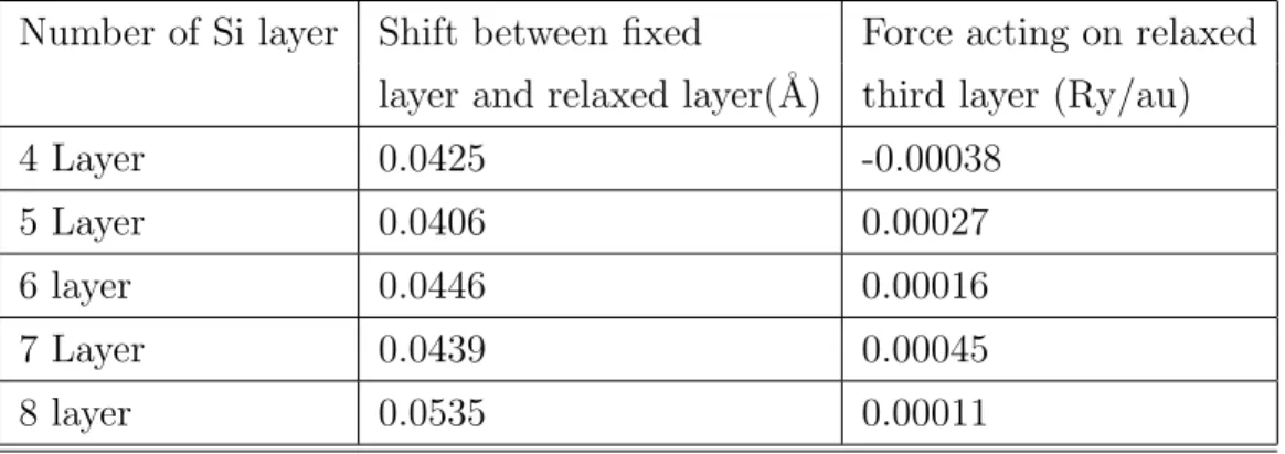
There are two important parameters in order to describe surfaces by a slab structure within a typical DFT calculation. The thickness of the vacuum region large enough to prevent interaction between the periodic image of the slab and the thickness of the slab that represents a silicon surface. The number of silicon layers is initially kept at four and then it is increased up to 8 layers. Throughout the calculation, the bottom two layers of Si are fixed and the other atoms are allowed to relax. After the relaxation calculations, it is observed that optimum number of layer within the slab can be set to five layers. Because, when the number of layer of the slab is larger than five layer, higher than 0.1˚A shift between fixed
Table 4.1: Relaxation of the slab structure with di↵erent number of layers Number of Si layer Shift between fixed Force acting on relaxed
layer and relaxed layer(˚A) third layer (Ry/au)
4 Layer 0.0425 -0.00038
5 Layer 0.0406 0.00027
6 layer 0.0446 0.00016
7 Layer 0.0439 0.00045
(a) 4 Si layer (b) 5 Si layer
(c) 6 Si layer (d) 7 Si layer (e) 8 Si layer
4.1.1
Dimer reconstruction
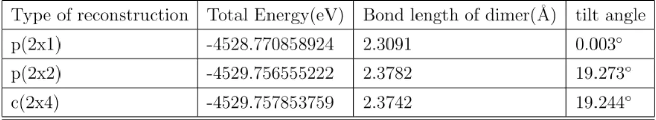
There are two dangling bonds per bulk truncated Si surface atom. These dangling bonds are energetically unstable. As a result, these surface atoms come closer to each other and form a dimer bond. [36, 37] This behaviour of surface atom is called dimerization. It is one type of silicon surface reconstruction. According to position of dimer, the Si (001) surface has three di↵erent surface reconstruction models. If the dimer is symmetric, the silicon surface is called p(2x1). If it is antisymmetric and this antisymmetric pattern is consistent with the neighbor dimer pattern, then the surface is called p(2x2). The other reconstruction type seen on silicon (001) is c(2x4). For this surface unit cell, the antisymmetric dimer must be consistent with cross neighbor dimer. Most energetically favorable dimer reconstruction is c(2x4) and second most favorable is p(2x2).
(a) p(2x1) reconstruction (b) p(2x2) reconstruction (c) c(2x4) reconstruction
Figure 4.2: Side view of silicon (001) (2x4) surface unitcell
(a) p(2x1) reconstruction (b) p(2x2) reconstruction (c) c(2x4) reconstruction
Table 4.2: Total energy of reconstructed silicon (001) surface
Type of reconstruction Total Energy(eV) Bond length of dimer(˚A) tilt angle p(2x1) -4528.770858924 2.3091 0.003 p(2x2) -4529.756555222 2.3782 19.273 c(2x4) -4529.757853759 2.3742 19.244
In these calculations, we have used our theoretical lattice constant for the bulk Si(5.46375˚A). A Monkhorst-Pack [27] mesh of 4x2x1 is used for Brillouin zone sampling. BZ integrations were performed using the Marzari-Vanderbilt spreading special point technique [32] with a smearing parameter of 0.01Ryd.
4.1.2
Surface and bulk states of Si (001)
The surface and bulk states of silicon are calculated using plane-wave pseudopo-tential method. In order to perform band structure of Si-bulk crystal, the vacuum area over Si (001) surface is filled with silicon atom. And energy values with re-spect to the surface BZ is calculated. By increasing the kz wavevector, the band
calculation is repeated for the same surface BZ. In order to obtain surface states, the energy values with respect to surface BZ are drawn at same graph. As shown the figure, the di↵erent states are observed at band energy calculation. Theses states are called surface states.
Figure 4.4: Schematic representation of surface Brillouin Zone for Si (001) p(2x1) surface unitcell
(a) Si (001) surface bulk terminated
(b) Si (001) surface symmetric dimer recon-struction
(c) Si (001) surface antisymmetric dimer re-construction
4.1.3
2+1 Dimer Vacancy on Si (001) surface
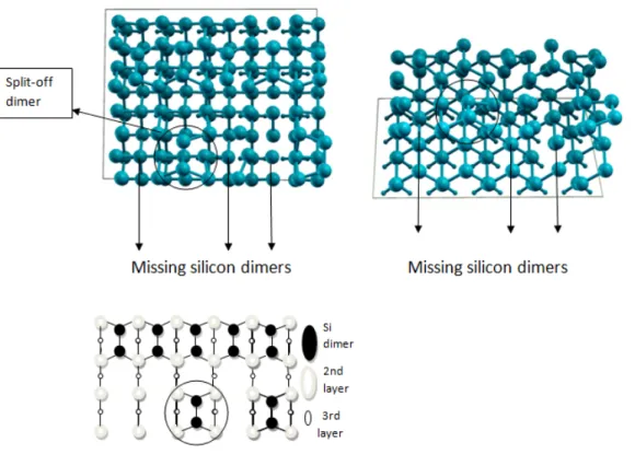
2+1 dimer vacancy is the generally observed defect structure during the nanowire growth mechanism. This type of defect has been also observed while deposing iridium atom on silicon surface. For that reason, defect analysis is needed to understand this phenomenon. In order to simulate this observed defect, 2 adjacent dimers are removed and the next dimer is allowed to stay and then one dimer is removed again. The resulting surface structure is 2+1. In order to calculate accurately, the number of layer is increased to 7 layer. After the system is relaxed, it is observed that the the surviving dimer are split o↵. This type of defect is also called as split-o↵ dimer defect. [38]
4.2
Iridium coverage on Si (001) surface
We have studied the adsorption of Ir atom on the Si(001) surface for 1/8, 1/4 and up to 1.5 ML coverage starting with the reconstructed p(2x4) surface unit cell.
4.2.1
0.125 ML coverage deposition over Si (001) surface
Before discussing Ir NW formation on Si(001), we have studied the single Ir atom adsorption over Si (001). We have placed one iridium into the di↵erent adsorption side of silicon. 1/8 ML iridium coverage corresponds to one iridium atom over eight silicon atoms. We have placed iridium atoms in several positions over the surface. We have chosen six di↵erent sites for Ir adsorption. In order to optimize the geometry, we used damped (quick-min Verlet) dynamics implemented in the PWscf code of Quantum ESPRESSO. After getting the total energy values of Si slab, we calculated binding energy as follows: The energy value of p(2x4) reconstructed Si (001) surface is subtracted from the total energy. The single iridium atom is also calculated and its energy value is subtracted from the total energy. Thus, we have found binding energy of slab as:
Figure 4.7: Schematic representation of p(2x4) Si (001) surface
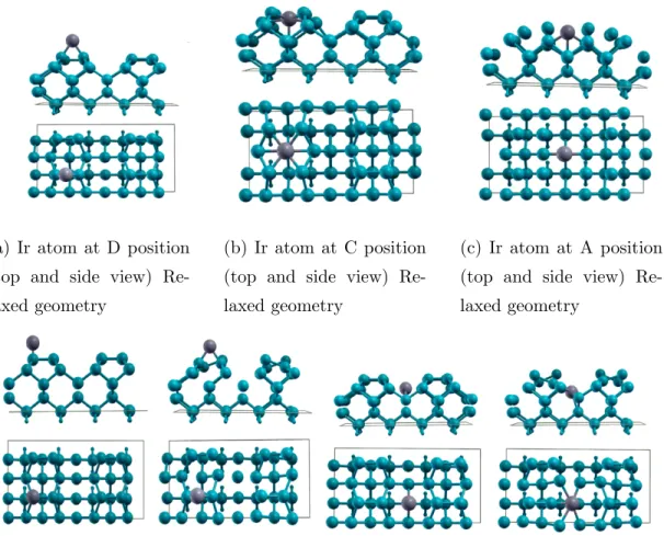
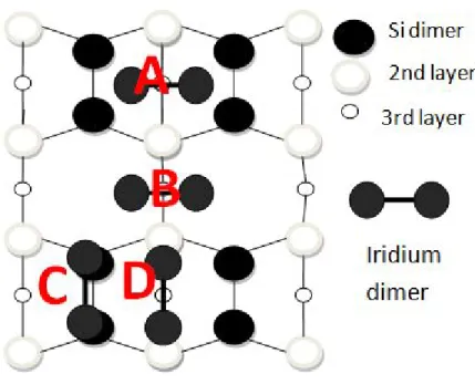
As seen on schematic representation of p(2x4) shown in fig 4.7, the probable iridium positions over Si (001) are labeled with capital letters A to F. The most stable configuration of iridium on surface is found when Ir atom is at configu-ration B, sitting over a hollow region between the dimers. When the relaxation is completed, Ir goes through inside the Si bulk and it tends to be merged into the fourth layer of silicon slab. This behavior of iridium is attributed that it wants to form bond with more silicon atoms. At the other configuration, there is not many adsorption sites enable iridium to connect with more than 2 silicon atoms. Although, this location gives higher binding energy, it is not preferable to form NW since after Ir is deposited over silicon terrace, the surface gets dis-torted and it reconstructs again. The same thing happens when the Ir atom is at configuration A. Moreover, it also gives lower binding energy. The second stable configuration and the one which gives higher binding energy is the adsorption over C-site position.
(a) Ir atom at D position (top and side view) Re-laxed geometry
(b) Ir atom at C position (top and side view) Re-laxed geometry
(c) Ir atom at A position (top and side view) Re-laxed geometry
(d) Ir atom at F position (top and side view) Unrelaxed geometry [Left Side] Relaxed ge-ometry [Right Side]
(e) Ir atom at B position (top and side view) Unrelaxed geometry [Left Side] Relaxed ge-ometry[Right Side]
(f) Ir atom at E position (top and side view) Unrelaxed geometry [Left Side] Relaxed ge-ometry [Right Side]
Table 4.3: Single Ir atom adsorption on p(2x4) Si (001) surface Adsortion position of Iridium Binding energy(eV)
A -7.9601 B -9.3613 C -8.3409 D -8.4051 E -7.2614 F -8.0398
4.2.2
0.25ML Iridium coverage on Si (001) surface
The 0.25 ML iridium coverage is simulated by deposing 2 Ir atoms at di↵erent adsorption site on Si (001) surface. As seen on the schema, the Ir dimers are itemized as capital letter A to D and their binding energies are shown on the table 4.4. The most stable configuration of Ir dimer induced silicon surface is seen when Ir dimers are aligned parallel to the dimer and they are placed into between them. The most drastic comment can be done while analyzing these results, the dimers don’t prefer to bond with dimer at the top position of silicon dimer. Rather than this behaviour, they stay between the bridge of dimers.
Figure 4.9: Schematic representation of position of adsorbed Ir dimer on p(2x4) Si (001) surface
Figure 4.10: Adsorbed Ir dimer on p(2x4) Si(001) [Left side] (Ir dimer at A) [right side] (Ir dimer at B)
Figure 4.11: Adsorbed Ir dimer on p(2x4) Si(001) surface [Ir dimer at C ] Left side [Ir dimer at D ] right side
The process to find the best structure of iridium silicide observed through the experiments is strongly dependent on how experimental conditions are im-plemented in ab initio calculations. Annealing is an important process which needs to be taken into account. Even though the DFT calculation is carried out at 0 K and the ground state energy is calculated, the analysis to estimate the optimized geometric structure is worthwhile to understand the experimental sit-uation. Since, during the experiment first the sample is kept at high temperature and then the temperature is lowered to room temperature leading to the NW for-mation, so the aim of this DFT based model is to understand how self-assembled nanowires grow at the surface. When the experimental STM images are analyzed, it is realized that the Si (001) surface accommodates dimer vacancy line. In order to make this kind of typical defect possible, the slab is modeled with vacancy Si atom and it is replaced with iridium atoms. This kind of ab-initio studies has been done to investigate the structure of self-assembly nanowire and the other important analysis is also find best match with experimental STM image. There-fore, all substitutional defects and vacany studies are applicable to understand
Table 4.4: Adsorbed Ir Dimer on p(2x4) Si (001) surface Position of Iridium dimer Binding Energy (eV)
A -8.2312
B -8.3272
C -6.6712
D -8.2995
the nature of surface.
In this part of thesis, silicon atoms are replaced with iridium atoms. The slab of unit cell is chosen as c(2x4), since this reconstruction type gives the most stable energy configuration. The atoms are enumarated from 1 to 8. The upper atom is colored as black and drawn bigger than the other dimer atom. The interesting conclusion which is derived from these calculations is that Ir atoms prefer bonding with silicon rather than itself. When the iridium atoms are substituted into positions labeled 1-2 , the substitution energy gives higher energy than the other configuration. It means, in order to obtain such as structure, the system needs to gain more energy than the other configurational possible structure. Therefore, bonding with Ir atom on Si (001) surface is not preferable when compared to bonding with Si atom.
Figure 4.12: Schematic represantation of Ir adsorption on c(2x4) Si (001) surface
Figure 4.13: Relaxed geometric image of substituted Ir atom over c(2x4) Si(001) surface [1-7] Left side [2-8] Right Side
Figure 4.14: Relaxed geometric image of substituted Ir atom over c(2x4) Si(001) surface [1-2] Left side [2-3] Middle [1-3] Right Side
Table 4.5: Substituted Ir atom and their substitution energy Position of Iridium Substitution energy (eV)
1-2 14.3188
2-3 13.8198
2-8 13.9083
1-7 14.1757
1-3 13.6556
4.2.3
The growth of Ir nanowire
Oncel et al. observed NW structure over Si (001) surface and these NWs are aligned parallel to Si dimer. In order to find similar NW formation over silicon, we have changed the surface unit cell of slab. p(4x2) is used for pure Si (001) surface and Ir atom is deposed over silicon surface which is parallel to the dimer direction.
Figure 4.15: Side view of Ir nanowire growth on p(4x2) Si(001) surface
As seen on figure 4.15, the Ir atoms are placed over Si(001) surface individually and their binding energy values are shown in table 4.6. The results show that Ir nanowires can be grown at surface. The first stable nanowire structure which is parallel to [110] direction is seen at figure 4.15. When eight Ir atoms are deposited on the surface, the hybrid molecules are composed over silicon. When iridium coverage is increased, the di↵erent kinds of NWs are generated over the surface. The rising of periodic iridium silicide can be interpreted as growth mechanism of iridium silicide phase diagram, since there are three known Ir-Si crystal structure and these crystals are obtained by deposing Ir atom over silicon surface [39]. Some of NWs are taken out of surface and their geometric structure is relaxed. These studies are summarized at section DFT study of iridium silicide NW
Table 4.6: Ir Nanowire growth mechanism on p(4x2) Si(001) surface Number of Iridium Binding energy(eV)
1 -8.3670 2 -8.3057 3 -8.3570 4 -8.1942 5 -8.3304 6 -8.6882 7 -8.5539 8 -8.8368 9 -8.8403 10 -9.2347 11 -9.1888 12 -9.0928
According to binding energy values of single Ir adsorption, iridium tends to be merged with Si atoms at terrace. Due to this reason, iridium atoms are substituted into the terrace of silicon bulk and their binding energy are calculated. After deposing four Ir atoms, the surface gets started to be reconstructed and
(a) Adsorbed Ir atom at terrace p(4x2) Si (001) surface [1-3] Ir Top and side view
(b) Adsorbed Ir atom at terrace p(4x2) Si (001) surface [4-6] Ir Top and side view
Figure 4.17: Adsorbed Ir atoms at terrace Si (001) surface
Table 4.7: Ir Nanowire growth mechanism at terrace Si(001) surface Number of Iridium Binding energy(eV)
1 -8.4089 2 -8.4572 3 -8.7570 4 -8.8328 5 -9.4456 6 -9.6291
Figure 4.20: Side view and top view of adsorbed 8 and 10 Ir atoms on p(2x4) Si(001) surface Side view [Left side] top view [Right side]
The last model for NW growth is to substitute Ir atoms between Si dimer positions one by one since probable iridium position between Si dimer positions is second most preferable configuration. That’s why, we have studied the between dimer position and keep on adding Ir atom in that direction. When 6 atoms are substituted over Si surface, the periodic NWs are formed and 2 of Ir atoms are buried into the bulk and four of them are observed at surface. This structure gives also very good binding energy. This formation can be model of NW; how-ever the direction of NW is di↵erent than the direction observed at STM image. When more Ir atoms are substituted, even though the binding energy is good, the geometric model cannot be described as NW.
Table 4.8: Iridium nanowire growth on p(2x4) Si (001) surface Number of Iridium Binding energy(eV)
1 -8.7604 2 -8.4772 3 -8.2744 5 -8.4331 6 -9.2174 8 -8.8379 10 -9.2191
4.2.4
DFT study of Ir Silicide Nanowire
After obtaining stable NW structure on Si surface, we have also tested possible nanowire structures for free-standing nanowires. This analysis can be attributed to how surface a↵ects the formation of nanowire. When the Ir silicide NWs are separated from the surface, some of them keep their position and the others show the di↵erent periodic patterns.
Figure 4.22: Unrelaxed 8 Ir atom per (4x2) unit cell(Left side), Relaxed geometric Ir-silicide nanowire (right side)
Figure 4.23: Unrelaxed 10 Ir atom per (4x2) unit cell (Left side), Relaxed geo-metric Ir-silicide nanowire (Right side)
Figure 4.24: Unrelaxed 12 Ir atom per (4x2) unit cell (Left side), Relaxed geo-metric Ir-silicide nanowire (right side)
Table 4.9: The total energy values of stable iridium silicide nanowire Number of Ir atom Total energy(Ryd)
6 -367.9401297266 8 -386.0776524619 10 -466.6463274061 12 -610.9583137248
4.2.5
Suggested nanowire model
According to Oncel’s tentative model, one dimer is taken out of surface and iridium is replaced with vacant dimer. When this model is used, it gives plausible binding energy, however the STM image doesn’t match with experimental image. Since, when iridium atom is substituted into silicon dimer, it tends to be buried into the Si bulk. That’s why the image which is thought as iridium cannot be observed at charge density.
(a) Side view of Oncel et al. model (b) top view of Oncel et al. model
Figure 4.26: Charge density contour of suggested nanowire model
As shown on figure 4.26, there are three dimers at Silicon (001) surface and the contour line of iridium charge density is seen at the middle of fourth layer silicon atoms.
(a) Side view of Oncel et al. model (b) top view of Oncel et al. model
Figure 4.28: Three dimensional STM image of Oncel et al. model
4.2.6
Ir-Si Nanowire model
Our model looks like Oncel et al.’s model; however, there is a di↵erence between them. The di↵erence comes from the behaviour of Ir atom, that is, it wants to be buried into the Si bulk. This tendency is also observed while implementing the tentative model of Nuri ¨Oncel et al. According to our model, the Si dimers must be still there and when they are kept on the surface, we observed that the Si dimers are rising up.
The five layer silicon system with fixed 2 layer may get trouble while imple-menting the position of buried iridium atom which is close to fixed layer. That’s why these calculations are repeated for 7 layer silicon slab. The result is consistent with the one previously we have found.
(a) Side view of Ir-Si NW model(7layer) (b) top view of Ir-Si NW model(7 layer)
Figure 4.30: Ir-Si Nanowire model (7layer) p(2x4)
(a) Side view of Ir buried model on p(2x2) Si (001) sur-face
(b) Top view of Ir buried model on p(2x2) Si (001) sur-face
Figure 4.32: Buried iridium on p(2x2) Si (001) surface
Band digram of buried iridium model is shown on figure 4.31. The bulk Si structure is set to p(2x2) and surface band diagram is plotted over the band diagram of bulk state.
Figure 4.33: 2 dimensional STM image with respect to Bias Voltage, distance of surface
Pseudo-STM images are generated by changing the parameter of sample bias voltage and the distance between the STM tip and surface layer. When the sample bias is set to -0.5V and the distance is adjusted as 1˚A, the generated pseudo-STM image provides the best agreement with the experimental STM image.
4.2.7
Buried iridium on Si (001) surface
We have also studied how binding energy is changing while increasing the coverage of buried Ir atom. As shown on table 4.10, the binding energy of Ir atom is decreasing while increasing the coverage of Ir atom and also when one Ir atom is placed into the terrace, the surface reconstructs and symmetric dimers are buckled.
(a) Buried 1 and 2 Ir on Si (001) surface (b) Buried 3 and 4 Ir on Si (001) surface
Figure 4.34: Buried iridium on Si (001) surface
Table 4.10: Iridium terrace
Number of Iridium Binding energy(eV)
1 -10.7340
2 -10.1863
3 -10.0672
Chapter 5
Conclusion
Nanowire growth mechanism is applicable under two main experimental tech-nique. These are bottom-up and top-down techniques. The most popular method is VLS technique based on supersaturation properties of catalytic liquid alloy. Recently, Nuri Oncel et al used self assembled nanowire growth technique by de-posing low coverage Iridium on Si(001). It has been used for last ten years. Its efficiency is compared with limit of lithography technique. Since, the main idea to produce nanowire should be thick and its size should be controlled under atomic resolution. This method is also known as epitaxially grown nanowire mechanism. Its one of the advantage is being easy to produce and its cost is lower than the other method. At 2003, Oguzhan G¨url¨u et al., used this technique to produce Pt nanowire on Ge(001); however the ab-initio study of Pt induced Ge (001) surface doesn’t verify the presence of Pt nanowire. It says that what is seen behind STM image is Ge nanowire. This analysis is also important to understand the behav-ior of Ir atom on Si(001) surface since Ir is one of platinum metal and its 5d fcc lattice structural properties are so close to platinum. Especially, its interaction with semiconductor is investigated in terms of tendency of orbital interaction.
In this thesis, using first-principle investigation, the iridium nanowire is stud-ied whether this one dimensional structure can be grown on silicon surface or not. Initially the single iridium atom adsorption at Si surface is analyzed. For this analysis, the binding energy term is used to compare the stability of composite
structures. While doing the calculation of binding energy, the single iridium and silicon atom energy is used. The methodology of analysis is based on that the iridium atom is assumed as gas phase. Its binding algorithm depends on its single energy calculation. The other analysis which is carried out to understand sta-bility of these structures is formation energy. According to this method, iridium initial phase depends on the cohesive energy of single Ir atom at fcc Ir bulk struc-ture. The main di↵erence is arisen from how iridium atom is composed before being deposed over silicon surface. Its analysis looks like the potential energy of electronic system. Binding energy gives reasonable analysis if the number of atom at silicon slab is kept as same amount through all calculation. Since while increasing iridium coverage, the binding energy of system is defined as amount per unit cell. However, if the number of silicon changes, there should be one invariant value which makes system depends on it. Thus, the stability of new composed structures can be compared with each other. Otherwise, we have to calculate the Gibbs energy of system. The other analysis to compare the exper-imental view with theoretical perception is based on how to interpret the STM image. According to Tersho↵-Ho↵mann theory, STM image can be analyzed by using local density of state calculation near Fermi energy. By adjusting the bias voltage at STM, it can be understood the electronic characteristic features of surface material. Thus, the system can be analyzed by calculating the LDOS of material near the Fermi level.
The second analysis is to check how surface gets reconstructed and what happens at surface when Ir coverage is increased. Hellmann-Feynman theorem helps us to understand the behavior of dangling bond under electric field arisen from charge polarization. In order to implement the relaxation technique at QUANTUM ESPRESSO software, damping method is used. Even though this algorithm is based on classical physics, it gives high accurate dimer angle and bond structure of silicon.
The silicon (001) surface is mostly investigated topic both experimental and theoretical. Its dimer structure has been discussed until 1995 since its STM im-age hasn’t verified its tilted dimer occurrence up to that time. After that not
di↵erences between these states and the small bais voltage is enough to change symmetrization of surface characteristic pattern from asymmetric dimer to sym-metric dimer.
After all analysis carried out to understand what is happening at silicon sur-face, we have drawn conclusion that the iridium tends to be buried into Si-bulk rather than adsorbing surface of silicon. When the Iridium coverage is increased, there are observed some NW structure at surface. These one dimensional com-positions are analyzed whether they can be sustainable structure without imple-menting silicon surface. After these structures are relaxed by keeping them peri-odic at one direction, we have modeled the possible NW structure. These models gives hope to be able to produce one dimensional Iridium-silicide nanowires at future. When they are investigated under experimental analysis, some of NW structures can be produced with the method of VLS (vapour-Liquid-Solid Tec-nique).
Figure 5.1: Calculated STM image of iridium silicide
As a consequence of analysis, the STM image is interpreted that what was seen at figure is not iridium. According to tentative model which is based on STM image, iridium atom is adsorbing at Si (001) surface by being replaced with Si dimer. After this model is implemented as probable structure, it was understood that if it was iridium, it should not be seen at surface. When the model is repeated by not removing the Si dimer at surface, it is apparently observed that the hill points observed at STM belongs to Si dimer rather than iridium atom.
between pseudo -STM image and experimental STM image and also verifies the observed surface symmetric pattern at LEED. Even through the number of layer is increased to 7 layer, the same pattern is observed at pseudo-STM. The low amount of coverage also supports accuracy of our model.
Bibliography
[1] R. E. Peierls, Quantum Theory of Solids. Oxford University Press, 1955. [2] G. Gr¨uner, Density Waves In Solids. Westview Press, 2000.
[3] J. M. Luttinger, “An exactly soluble model of a many-fermion system,” vol. 4, no. 9, pp. 1154–1162, 1963.
[4] J. V. Barth, G. Costantini, and K. Kern, “Engineering atomic and molecular nanostructures at surfaces,” Nature, vol. 437, no. 7059, pp. 671–679, 2005. [5] O. Gurlu, O. A. O. Adam, H. J. W. Zandvliet, and B. Poelsema,
“Self-organized, one-dimensional Pt nanowires on Ge(001),” Applied Physics Let-ters, vol. 83, no. 22, pp. 4610–4612, 2003.
[6] N. Oncel and D. Nicholls, “Iridium silicide nanowires on Si(001) surfaces,” Journal of Physics: Condensed Matter, vol. 25, no. 1, p. 014010, 2013. [7] A. A. Stekolnikov, J. Furthm¨uller, and F. Bechstedt, “Pt-induced nanowires
on Ge(001): Ab initio study,” Physical Review B, vol. 78, no. 15, p. 155434, 2008.
[8] “Formation of Pt-induced Ge atomic nanowires on Pt / Ge(001):,”
[9] D. E. P. Vanpoucke and G. Brocks, “Density functional theory study of Pt-induced Ge(001) reconstructions,” Physical Review B, vol. 81, no. 3, p. 035333, 2010.
![Figure 1.1: STM image of the Ir silicide nanowires (Reproduced from reference [6])](https://thumb-eu.123doks.com/thumbv2/9libnet/5545194.107970/16.918.343.664.170.474/figure-stm-image-ir-silicide-nanowires-reproduced-reference.webp)
![Figure 2.2: Schematic illustration of supercell geometry for a surface of a bulk solid Reproduced from reference [26]](https://thumb-eu.123doks.com/thumbv2/9libnet/5545194.107970/34.918.277.700.254.830/figure-schematic-illustration-supercell-geometry-surface-reproduced-reference.webp)